Active Matrix Substrate, Method for Fabricating Active Matrix Substrate, Display Device, Liquid Crystal Display Device, and Television Device

a technology of active matrix substrate and substrate, which is applied in the direction of optics, instruments, electrical equipment, etc., can solve the problems of pixel in which a short circuit has occurred, inability to repair, and likewise occur point defects, so as to improve production yields

Active Publication Date: 2008-01-03
SHARP KK
View PDF13 Cites 32 Cited by
  • Summary
  • Abstract
  • Description
  • Claims
  • Application Information

AI Technical Summary

Benefits of technology

[0043] According to the present invention, a point defect in an AM substrate can be repaired. This can improve production yields.

Problems solved by technology

Thus, the pixel in which a short circuit has occurred is found as a point defect on a display image.
Furthermore, also when poor etching or poor photolithography cause a short circuit between the data signal line 53 and the upper storage capacitor electrode 55a which are formed in the same process step due to defects, such as an unnecessarily left part 98 of a film, a point defect likewise occurs and cannot be repaired.
As a result, the display quality is significantly affected by the bright dot.
Accordingly, a defective pixel has come to be large enough to be unignorable from the viewpoint of the display quality.
In this technique, a pattern becomes complicated by dividing one pixel into a plurality of subpixels, resulting in the reduced aperture ratio of the pixel.
More specifically, even when a pixel is divided into, for example, two subpixels, the existence of conductive foreign particles or a pin hole in a part of an insulating layer between a storage capacitor line (lower storage capacitor electrode) and an upper storage capacitor electrode causes a short circuit therebetween.
As a result, the display quality is insignificantly affected by the point defect.
In a case where a current leakage failure is caused, two subpixel electrodes 51L and 51R sharing a storage capacitor (common) line 57 become electrically continuous, resulting in combined defects.
In view of the above, a subpixel of one (second pixel) of the adjacent pixels is nonenergized, leading to a point defect.
The AM substrate in which a pixel is divided into a plurality of subpixels may cause a current leakage failure between adjacent upper storage capacitor electrodes 55La and 55Ra, resulting in an increase in the possibility of bringing about a point defect.

Method used


Image

  • Active Matrix Substrate, Method for Fabricating Active Matrix Substrate, Display Device, Liquid Crystal Display Device, and Television Device
  • Active Matrix Substrate, Method for Fabricating Active Matrix Substrate, Display Device, Liquid Crystal Display Device, and Television Device
  • Active Matrix Substrate, Method for Fabricating Active Matrix Substrate, Display Device, Liquid Crystal Display Device, and Television Device

Examples


embodiment 1

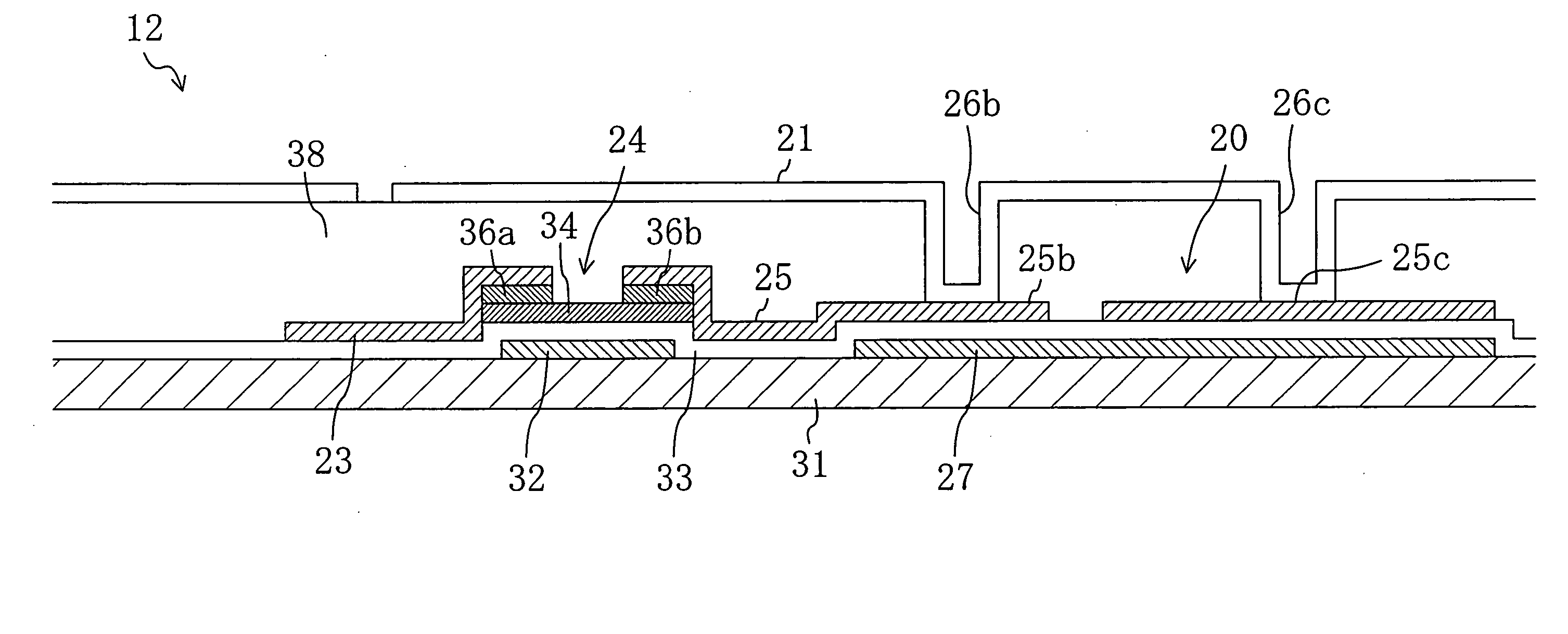
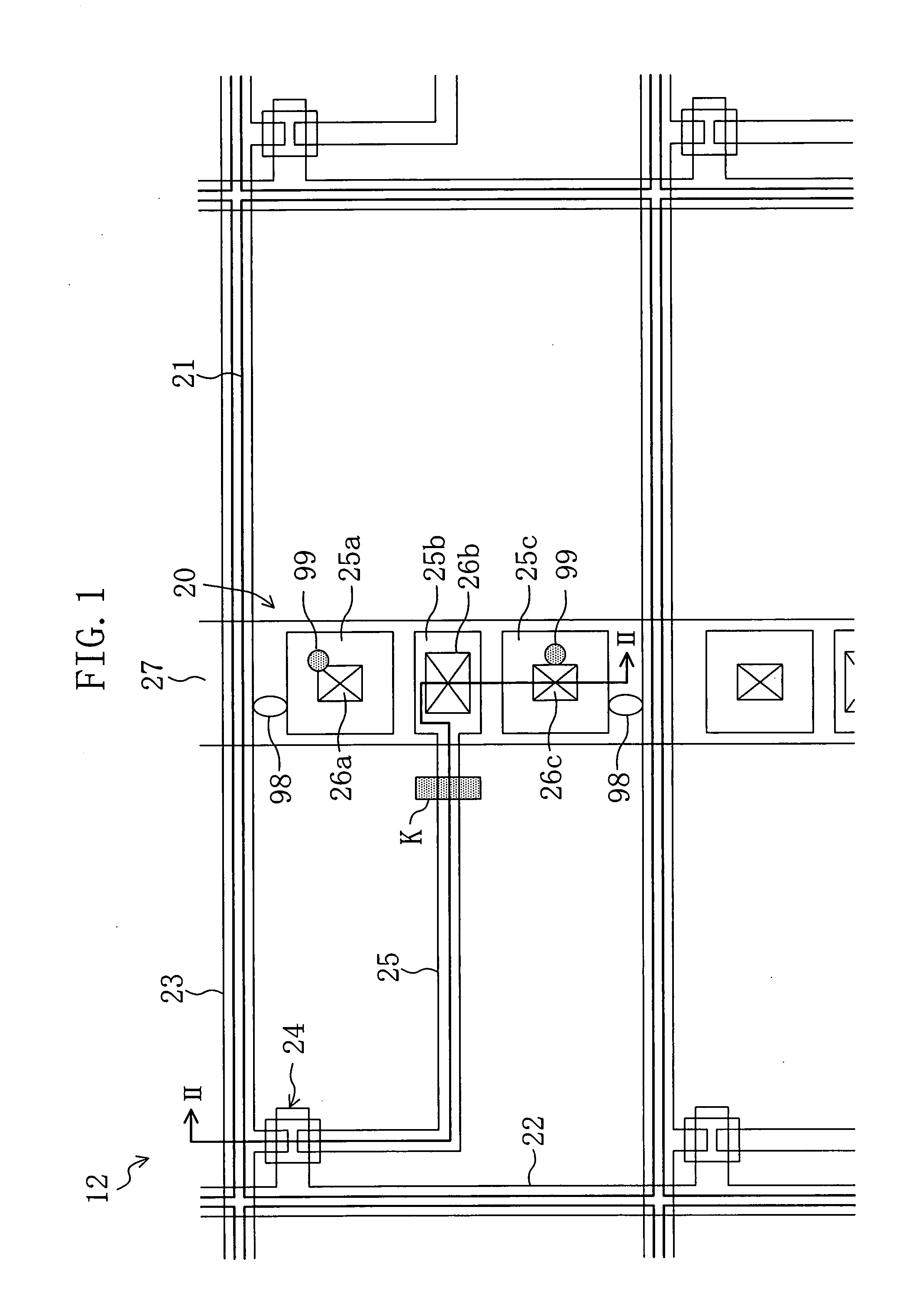
[0107]FIG. 3 is a plan view schematically illustrating an AM substrate 12a of this embodiment. FIG. 4 is a cross-sectional view taken along the line IV-IV in FIG. 3. The AM substrate 12a of this embodiment takes on a Cs-on-Common structure in which a storage capacitor line is formed as a lower electrode of a storage capacitor element. The AM substrate 12a of this embodiment is configured such that a pixel is divided into two subpixels and each adjacent pair of pixels share a storage capacitor line.

[0108] Each subpixel herein is the smallest unit of display. Two or more subpixels which are selected by a scanning signal supplied to the same scanning signal line and a data signal supplied to the same data signal line and to which the same data signal is fed form one pixel. Furthermore, three pixels corresponding to R, G and B form one picture element. A pixel (or subpixel) region of an AM type liquid crystal display device is defined by a pixel electrode (or a subpixel electrode) and ...

embodiment 2

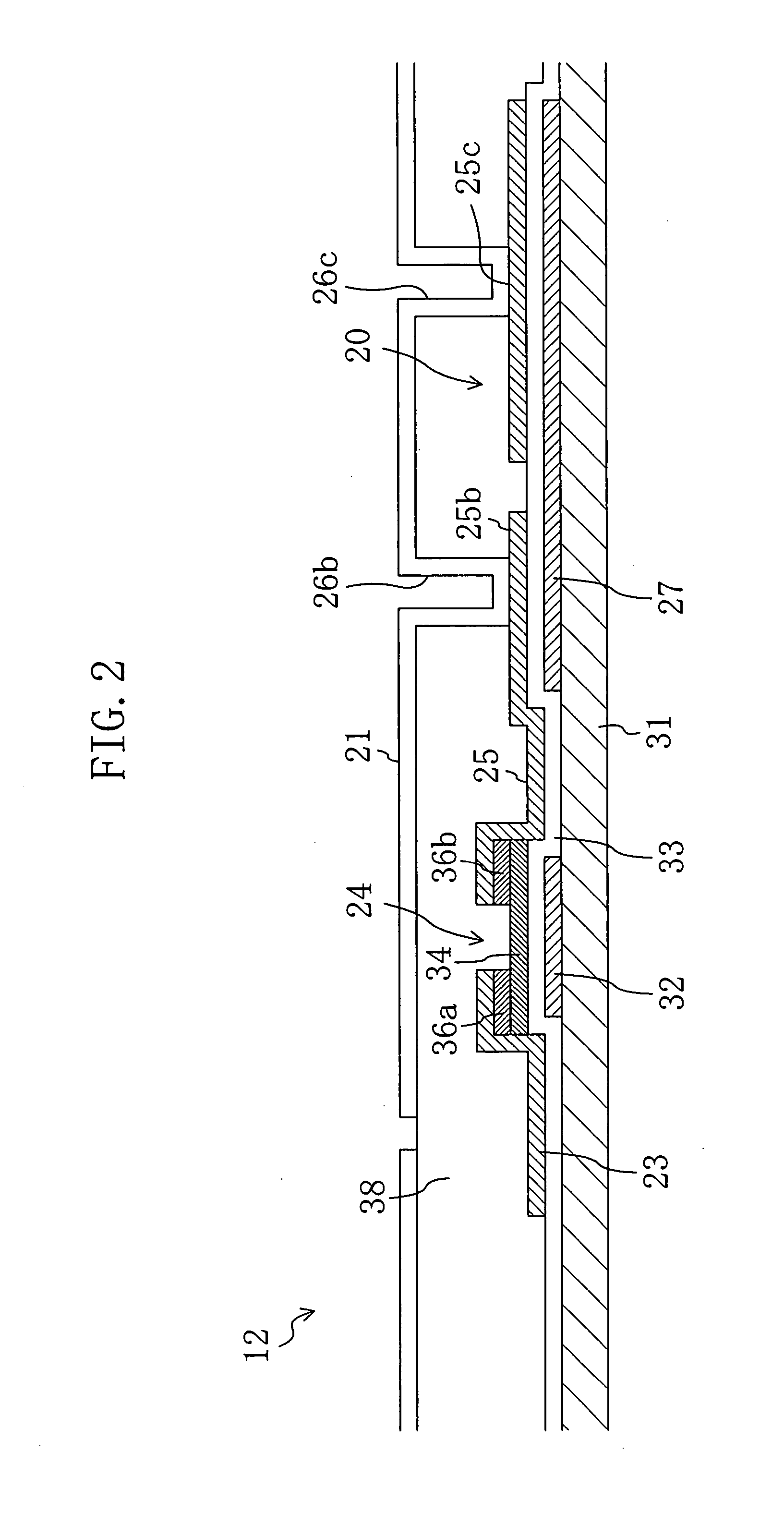
[0127] The AM substrate 12a of the first embodiment is set such that the total area (first area) of regions of the storage capacitor line 27 on which the upper storage capacitor electrodes 25a and 25c connected to the connection electrodes 25R and 25L are placed is larger than that (second area) of regions thereof on which the upper storage capacitor electrodes 25b and 25d prevented from being connected to the connection electrodes 25R and 25L are placed.

[0128] It may be more difficult to connect the subpixel electrodes 21R and 21L via the contact holes 26b and 26d to the upper storage capacitor electrodes 25b and 25d with excellent coverage than to connect the subpixel electrodes 21R and 21L via the contact holes 26a and 26c to the upper storage capacitor electrodes 25a and 25c with excellent coverage. Furthermore, the contact resistance between a metal film forming upper storage capacitor electrodes and containing aluminum or any other metal and a film forming the subpixel electr...

embodiment 3

[0132] For the AM substrate 12b of the second embodiment, as illustrated in FIG. 11, the upper storage capacitor electrodes 25a and 25b corresponding to the right one (first subpixel) of two subpixels included in the first pixel located at the left side of the storage capacitor line 27 (the left one of the two subpixels is only partially shown) are arranged to be symmetrical to the upper storage capacitor electrodes 25c and 25d corresponding to the left one (second subpixel) of two subpixels included in the second pixel located at the right side of the storage capacitor line 27 (the right one of the two subpixels is only partially shown). In other words, the upper storage capacitor electrode 25a associated with the first subpixel and connected to the connection pixel 25R is adjacent to the upper storage capacitor electrode 25c associated with the second subpixel and connected to the connection electrode 25L in a direction crossing the direction in which the storage capacitor line 27...


PUM

PropertyMeasurementUnit
widthaaaaaaaaaa
thicknessaaaaaaaaaa
thicknessaaaaaaaaaa

Abstract

An active matrix substrate includes a substrate, a TFT formed on the substrate, a storage capacitor element formed on the substrate, an interlayer insulating film covering the storage capacitor element, and a pixel electrode formed on the interlayer insulating film. The storage capacitor element includes a storage capacitor line, an insulating film formed on the storage capacitor line, and two or more storage capacitor electrodes opposed to the storage capacitor line with the insulating film interposed therebetween. The two or more storage capacitor electrodes are electrically connected via associated contact holes formed in the interlayer insulating film to the pixel electrode and electrically continuous with a drain electrode of the TFT.

Description

TECHNICAL FIELD [0001] The present invention relates to active matrix substrates, methods for fabricating active matrix substrates, display devices, liquid crystal display devices, and television devices, and more particularly relates to active matrix (hereinafter, referred to also as “AM”) substrates, for example, having pixels each provided with a thin-film transistor for driving a liquid crystal layer and a storage capacitor element, and AM type liquid crystal devices each including such an AM substrate. BACKGROUND ART [0002] AM substrates have been widely used for AM type display devices, such as liquid crystal display devices and EL (electroluminescence) display devices. A known AM type liquid crystal display device using such an AM substrate includes a plurality of scanning signal lines formed on the substrate, a plurality of data signal lines crossing the scanning signal lines, thin-film transistors (hereinafter, referred to also as “TFTs”) located at the intersections of the...

Claims


Application Information

Patent Timeline
Patent Type & Authority Applications(United States)
IPC IPC(8): G02F1/1343H01L21/84
CPCG02F1/136259G02F1/136213
Inventor YAGI, TOSHIFUMINODA, TOMOKITSUBATA, TOSHIHIDETAKEUCHI, MASANORIENDA, KENJI
Owner SHARP KK
Why Eureka
Try Eureka