
Method for in-line monitoring a lens controller of a photolithography system

a technology of photolithography and lens controller, which is applied in the direction of photomechanical treatment, printing, instruments, etc., to achieve the effect of keeping the process cost low

Inactive Publication Date: 2008-01-03
TEXAS INSTR INC
View PDF3 Cites 2 Cited by
  • Summary
  • Abstract
  • Description
  • Claims
  • Application Information

AI Technical Summary

Benefits of technology

[0006] The present invention provides a method for in-line monitoring a lens controller of a photolithography system by means of which a possible failure of the lens controller is immediately detected without significantly increasing processing costs.
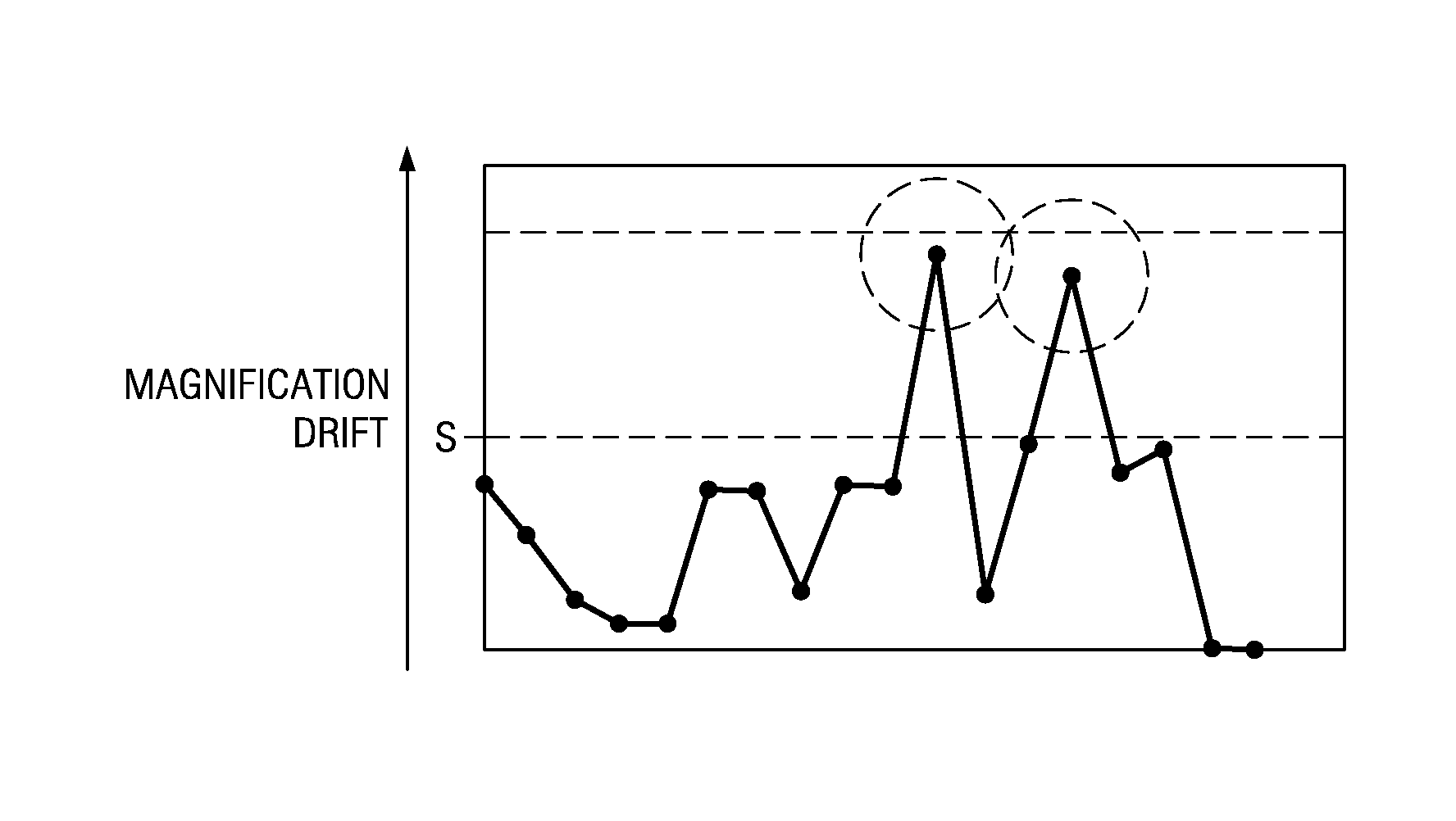
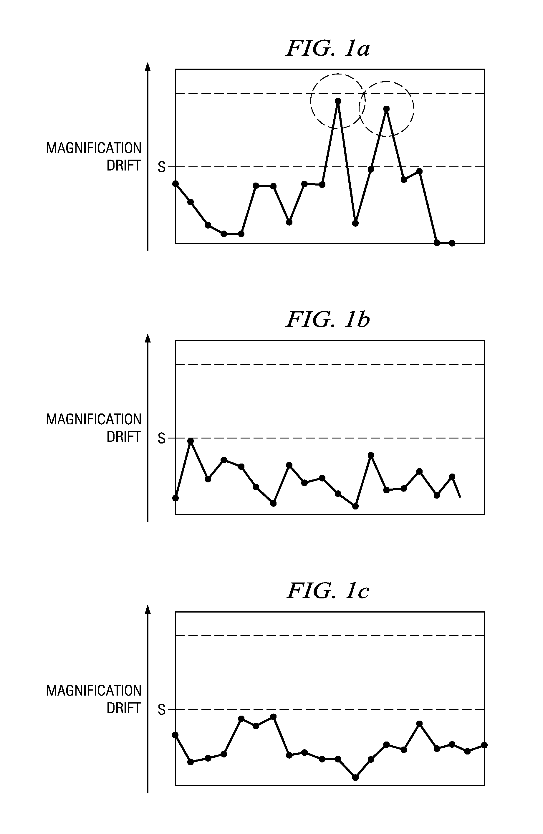
[0008] According to an embodiment of the invention the shot magnification value is determined in connection with overlay measurement, i.e. the measurement of how accurately a layer aligns with respect to another layer located above or below that layer. For that purpose the overlay deviation is measured between two overlying layers and, based on the overlay deviation, among other parameters, a shot magnification value is determined. A variation of the shot magnification values of the wafers of a lot exceeding a first predetermined value is an indicator for a malfunction of the lens controller. The shot magnification from wafer to wafer is a by-product of the overlay measurement so that monitoring of the lens controller according to the method of the present invention is based on available lot data and thus keeps the process costs low.

Problems solved by technology

In addition, the determination of the shot magnification is part of a typical exposure process so that determination of these values is not coupled with additional efforts that would increase the costs.

Method used


Image

  • Method for in-line monitoring a lens controller of a photolithography system
  • Method for in-line monitoring a lens controller of a photolithography system

Examples


Embodiment Construction

[0011] The structure and functioning of a photolithography system is known from prior art and shall not be discussed here in detail. A typical photolithography system comprises a reticle on which a circuit pattern is formed and a device known as a “stepper” for focusing the reticle pattern image on a wafer. The stepper contains a set of lenses (which is here referred to as “a lens”) to focus the reticle pattern image on a wafer. The light passing through the lens heats the lens, thereby expanding the lens and changing its focal length and magnification. A lens controller compensates for these effects so that the reticle pattern image is projected on the processed wafer in focus and with a predetermined magnification.

[0012] The reticle pattern image is focused on a light sensitive photoresist layer formed on the wafer. The photoresist is developed so that an image of the pattern is left on the wafer. The photoresist may then be used as a mask for the deposition or removal of materia...


PUM


Abstract

A method for in-line monitoring a lens controller of a photolithography system in which a plurality of wafers of a lot are processed in succession and which includes a lens for projecting a mask pattern on the wafers and a lens controller for correcting magnification of the lens includes the steps of printing a circuit pattern on each of the wafers of the lot by projecting a mask pattern on the wafers by means of a lens, determining a shot magnification value for a sample of the wafers, and continuously monitoring the variation of the shot magnification values, wherein a variation of the shot magnification values exceeding a first predetermined value indicates a failure of the lens controller.

Description

CROSS-REFERENCE TO RELATED APPLICATIONS [0001] This application claims priority of German Patent Application Serial No. 10 2006 009 703.3, filed Mar. 2, 2006 and the benefit of U.S. Provisional Application Ser. No. 60 / 882,388, filed Dec. 28, 2006.TECHNICAL FIELD [0002] The present invention relates to a method for in-line monitoring a lens controller of a photolithography system in which a plurality of wafers are processed in succession, wherein the photolithography system comprises a lens for projecting a mask pattern on the wafers and a lens controller for correcting lens heating effects and, in particular, magnification and focus of the lens. [0003] In a photolithography system a mask pattern is imaged by means of a lens on a photosensitive layer which is present on the wafer. In order to form well-defined patterns it is important that the mask pattern is imaged in focus on the photosensitive layer and with an accurately determined magnification. During the exposure process the l...

Claims


Application Information

Patent Timeline
IPC IPC(8): G03B27/42
CPCG03F7/70258G03F7/70891G03F7/70616G03F7/70525
Inventor SCHWEKENDIEK, HOLGERBIESE, GERNOTURBAN, ALEXANDER
Owner TEXAS INSTR INC
Learn More