Load compensated switching regulator

a switching regulator and load compensation technology, applied in the direction of power conversion systems, instruments, process and machine control, etc., can solve the problems of less desirable mode of operation than a floating boot supply, less pins available, and more wasted power

Active Publication Date: 2008-01-10
INTERSIL INC
View PDF1 Cites 36 Cited by
  • Summary
  • Abstract
  • Description
  • Claims
  • Application Information

AI Technical Summary

Benefits of technology

[0018]The above described embodiment employs hysterisis: An increasing load current causes a switch to the higher supply voltage at a higher load current level than a decreasing load current causes a switch to

Problems solved by technology

This mode of operation is less desirable than a floating BOOT supply, as it requires higher voltage components and generates more wasted power.
This might be due to a lack of pins available on an IC, for instance, when D1 is integrated within the IC.

Method used


Image

  • Load compensated switching regulator
  • Load compensated switching regulator
  • Load compensated switching regulator

Examples


Embodiment Construction

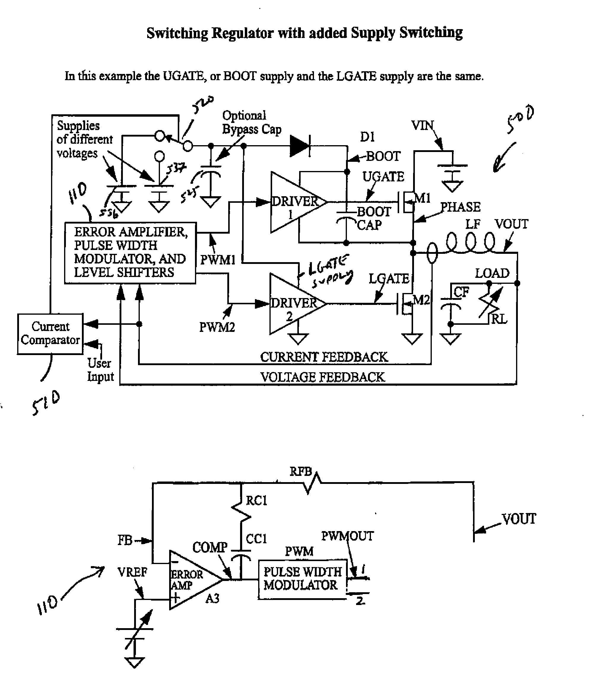
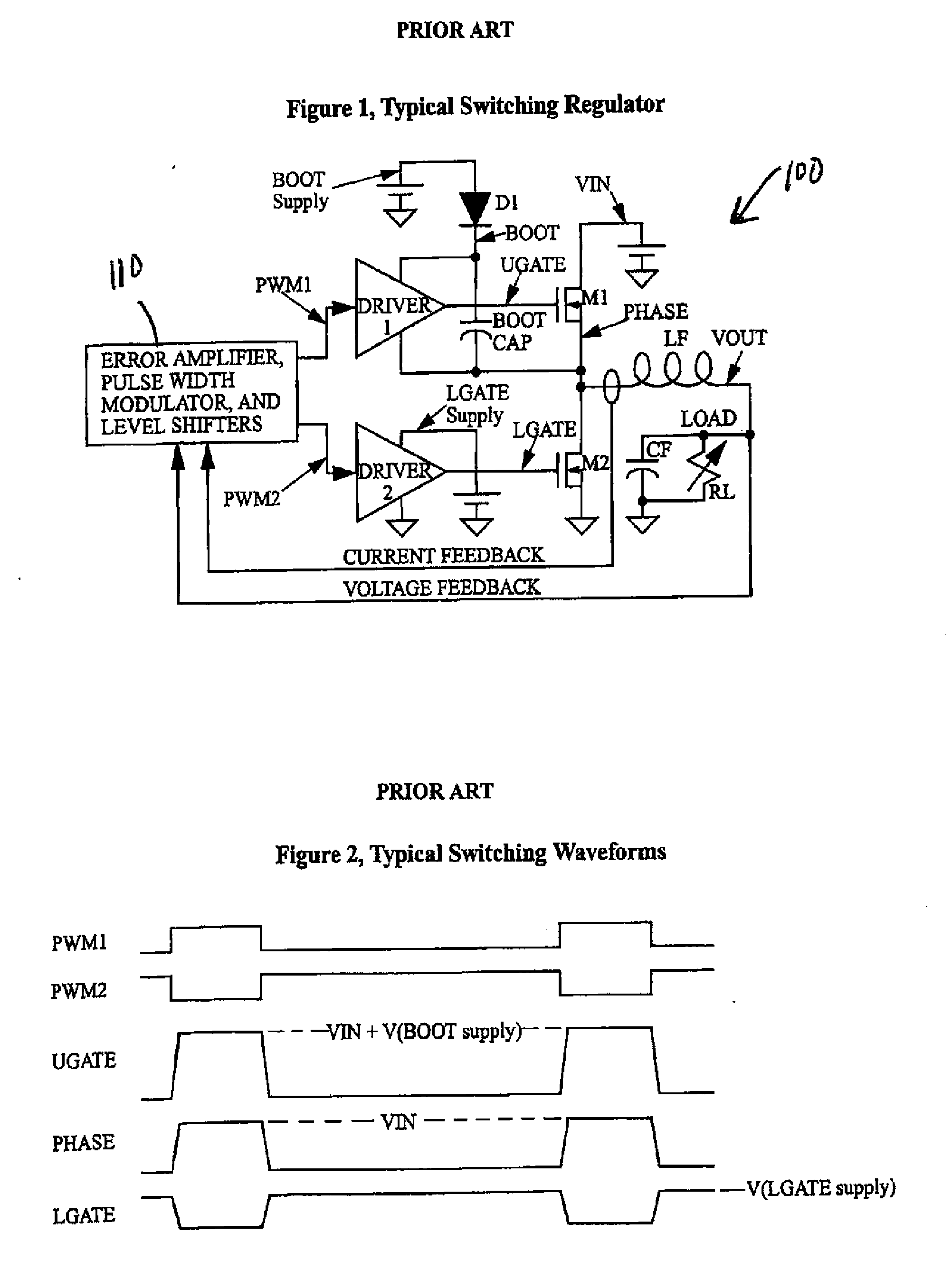
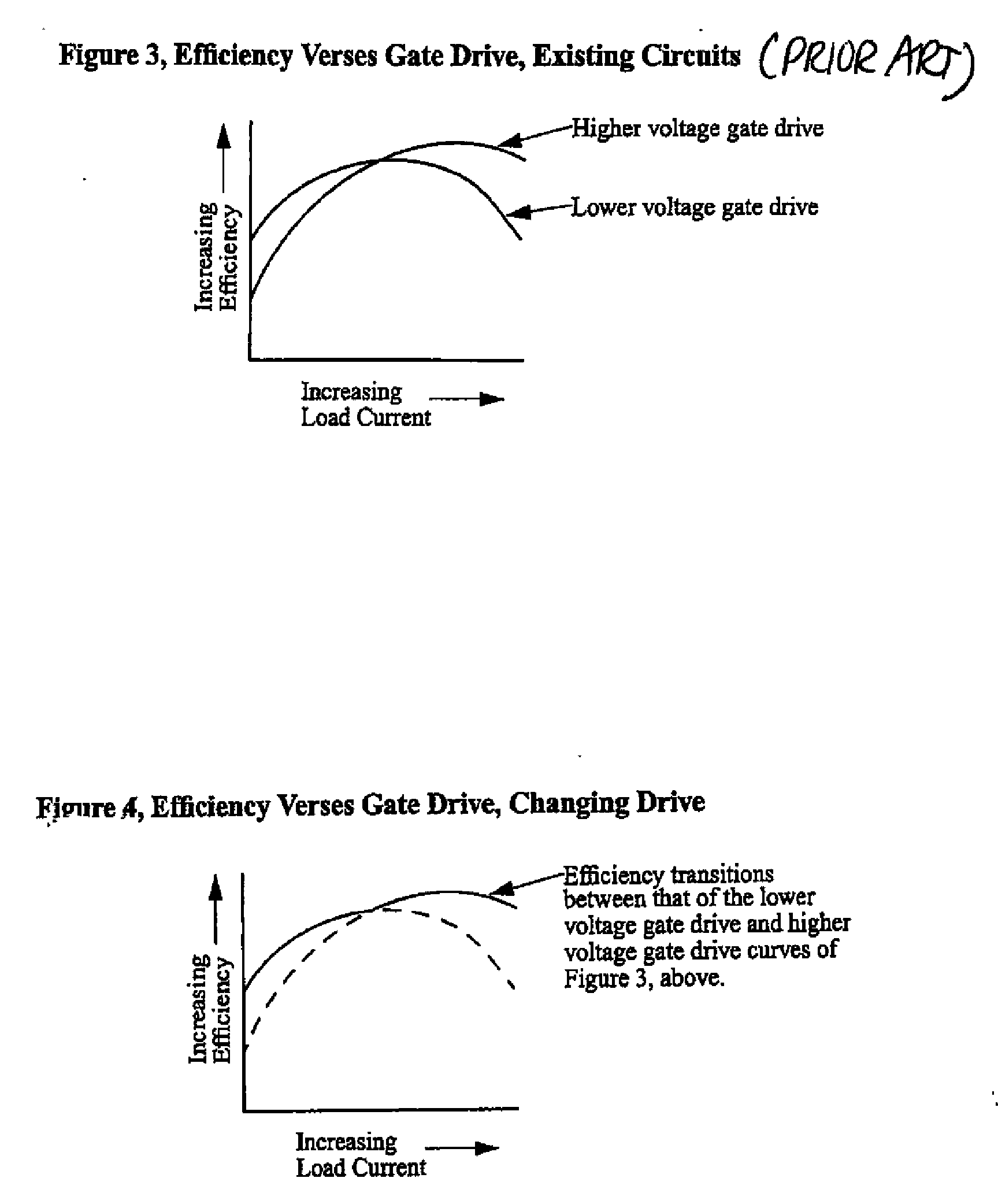
[0032]A load compensated voltage regulator is described herein that detects the load current and uses the load current, and optionally other measurables of circuit characteristics, to modulate the gate driver voltage supply level. Higher gate driver supply voltages are provided at higher load currents, and lower gate driver supply voltages at lower load currents. Such supply switching improves the power efficiency of the switching regulator. The gate driver voltage supply regulation may be implemented through analog circuitry, or primarily digital circuitry. Although the invention as described herein is shown as being based on CMOS circuitry, those having ordinary skill in the art will appreciate the invention can be realized in bipolar or BIMOS designs.

[0033]The error amplifier, pulse width modulator (PWM), and level shifters for the regulators according to the invention described herein are not part of the present invention, but as noted above are described herein for completeness...


PUM


Abstract

A load compensated voltage regulator comprises a chip including a control section having an error amplifier, a pulse width modulator (PWM), the PWM outputting at least one driver control signal. At least one driver has an input coupled to receive the driver control signal. An output stage includes at least one output transistor having an input coupled to an output of the driver. The output transistor drives an inductor in series with a grounded capacitor, wherein an output of the regulator (VOUT) is at a node between the inductor and the capacitor, wherein VOUT generates a load current across a load when connected across the capacitor. A feedback connector is provided for feeding back a feedback signal representative of the load current to circuitry for outputting a gate driver voltage supply control signal based on at least reference level and the feedback signal. A connector couples at least one power supply to the driver through a switch or a second regulator. The gate driver voltage supply control signal is coupled to the switch or regulator, wherein the gate driver voltage supply control modulates a voltage level of the gate driver voltage supply between at least two different levels based on the load current.

Description

CROSS-REFERENCE TO RELATED APPLICATIONS[0001]This application claims the benefit of Provisional Application No. 60 / 819,161 entitled “LOAD COMPENSATED SWITCHING REGULATOR” filed on Jul. 7, 2006, which is incorporated by reference in its entirety into the present application.FIELD OF THE INVENTION[0002]The invention relates to closed loop voltage regulators, and more particularly to switching regulators having networks for improving power efficiency.BACKGROUND OF THE INVENTION[0003]FIG. 1 shows a typical switching regulator 100, emphasizing the output section, while FIG. 2 shows pertinent switching waveforms for regulator 100. The control section of the regulator, not shown in detail, typically comprises an error amplifier with feedback components, a modulator circuit, and level shifters, collectively 110, to translate the resulting desired pulse widths into signal levels suitable for the Drivers 1 and 2. A reference voltage is typically applied to the non-inverting input of error amp...

Claims


Application Information

Patent Timeline
IPC IPC(8): G05F1/00
CPCH02M2001/0022H02M1/08H02M1/0022
Inventor ISHAM, ROBERT H.
Owner INTERSIL INC
Why Eureka
Try Eureka