Waveguide structure and optical device

a waveguide and optical device technology, applied in the direction of optical waveguide light guides, instruments, nanotechnology, etc., can solve the problems of difficult manufacturing and achieve the effect of easy manufacturing

Inactive Publication Date: 2008-01-17
HAMAMATSU PHOTONICS KK
View PDF0 Cites 11 Cited by
  • Summary
  • Abstract
  • Description
  • Claims
  • Application Information

AI Technical Summary

Benefits of technology

[0008]Thus an object of the present invention is to provide a waveguide structure and an optical device that can be manufactured easily and are longer in the propagation distance of surface plasmon waves.
[0038]With the waveguide structure and the optical device according to the present invention, manufacture is easy and surface plasmon waves can be propagated over a longer distance.

Problems solved by technology

L364-L366, because a metal is used, processing is difficult and as a result, manufacturing is difficult.

Method used


Image

  • Waveguide structure and optical device
  • Waveguide structure and optical device
  • Waveguide structure and optical device

Examples


first embodiment

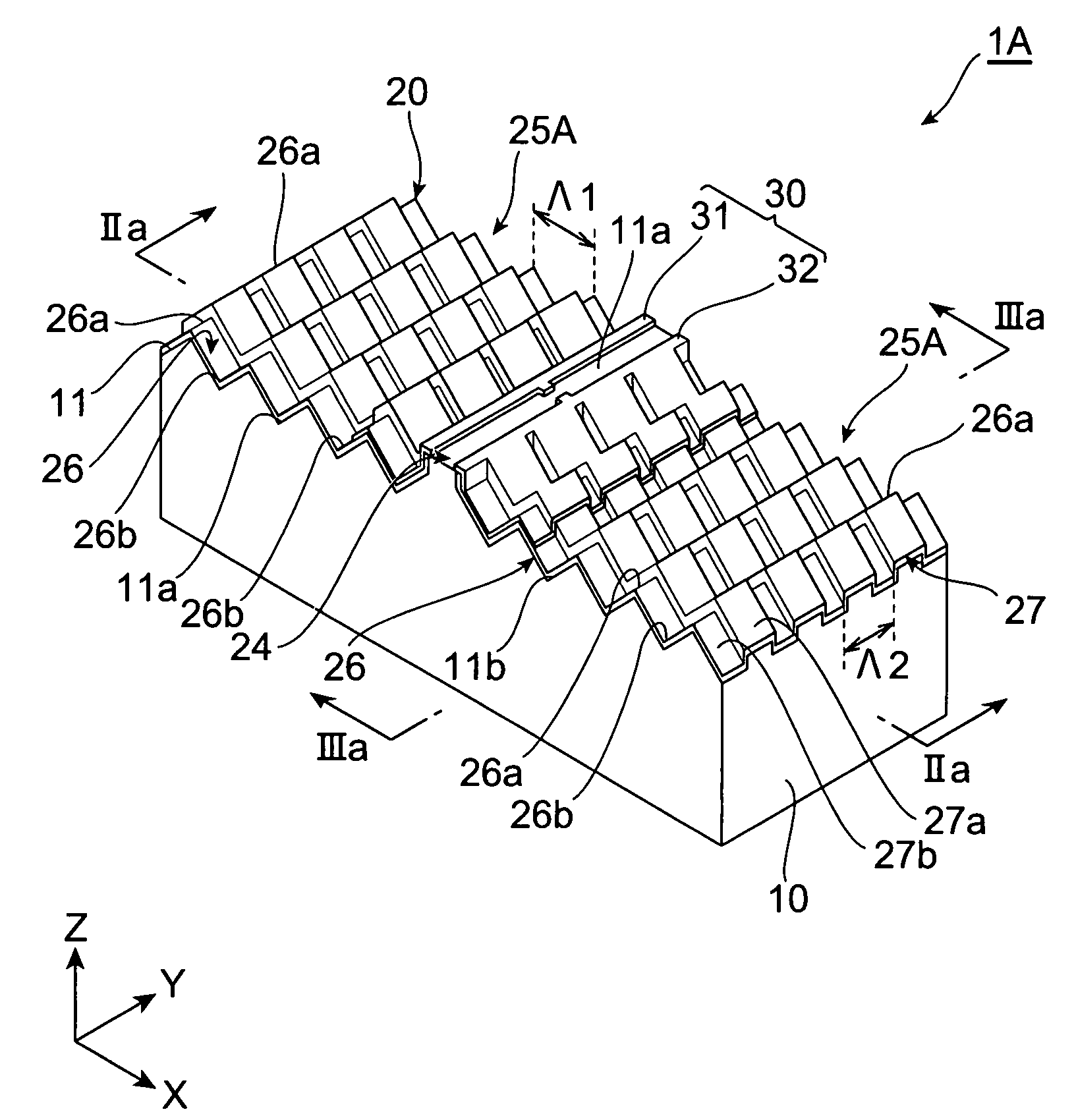
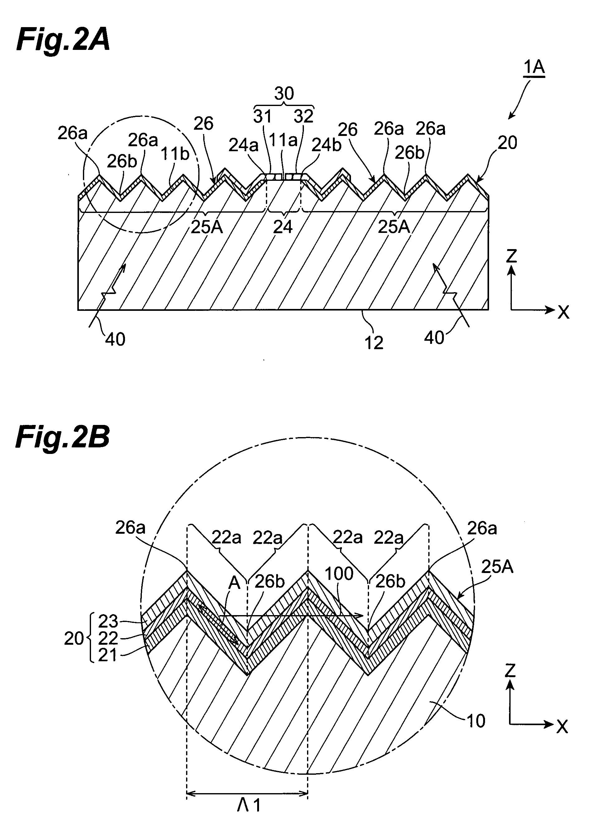
[0076]FIG. 1 is a perspective view of an embodiment of an optical device according to the present invention. FIG. 2A shows a sectional view taken on line IIa-IIa of FIG. 1. FIG. 2B shows a partially enlarged view of FIG. 2A. FIG. 3A shows a sectional view taken on line IIIa-IIIa of FIG. 1. FIG. 3B shows a partially enlarged view of FIG. 3A. An embodiment of a waveguide structure according to the present invention is applied to the optical device 1A. The optical device 1A shown in FIG. 1 is a THz light receiving element for detecting THz waves, which are light components of wavelengths in a range of 30 μm to 1000 μm (or oscillation frequencies in a range of 1.9×10¹² to 6.3×10¹³ (1 / sec)).

[0077]The optical device 1A includes a semiconductor substrate 10, which can propagate THz waves and is formed, for example, of GaAs, and a layer-like waveguide 20 (waveguide structure, quantum well structure) is laminated on the semiconductor substrate 10. In the description that follows, a laminatio...

second embodiment

[0115]FIG. 12 is a perspective view of a second embodiment of an optical device according to the present invention. A main difference in terms of arrangement of the optical device 1B with respect to the optical device 1A is that whereas the periodic structure portion 25B of the waveguide 20 has the uneven pattern 26 in the X-axis direction, there is no uneven pattern in the Y-axis direction. The optical device 1B shall now be described mainly in regard to this point.

[0116]The aperture 24 (focusing portion) is formed in the waveguide 20 laminated onto the semiconductor substrate 10 of the optical device 1B and the regions at both sides of the aperture 24 are the periodic structure portions 25B. The periodic structure portions 25B have the uneven pattern 26, having the period Λ1 and functioning as the surface plasmon wave generating portion.

[0117]The optical device 1B is formed is manufactured for example as follows. First, the steps illustrated in FIGS. 5A to 8B of the manufacturing ...

third embodiment

[0119]FIG. 13 is a perspective view of a third embodiment of an optical device according to the present invention. FIG. 14 is a sectional view taken on line XIV-XIV of FIG. 13.

[0120]The optical device 1C is a THz wave generating element that generates a THz wave. Main differences in terms of arrangement between the optical device 1C and the optical device 1B of the second embodiment are that with the optical device 1C, a semiconductor layer 50 is laminated further on the waveguide 20, which is laminated onto the semiconductor substrate 10, and a THz generating portion 60 is disposed on a top surface 51 of the semiconductor layer 50. The optical device 1C shall now be described mainly in regard to this point. The alternate long and short dash lines in FIGS. 13 and 14 schematically indicate a boundary between the semiconductor substrate 10 and the semiconductor layer 50 for the sake of description. Also for illustration of the arrangement of the waveguide 20, the waveguide 20 is indic...


PUM


Abstract

There is disclosed a waveguide structure that propagates surface plasmon waves, comprising: a quantum well structure, disposed on a semiconductor substrate; wherein the quantum well structure has a quantum well layer, in turn having an intersecting region that intersects a hypothetical plane substantially orthogonal to an alignment direction of the quantum well structure with respect to the semiconductor substrate, and a real part of a dielectric constant of the quantum well structure is negative for THz waves of a predetermined wavelength.

Description

BACKGROUND OF THE INVENTION[0001]1. Field of the Invention[0002]The present invention relates to a waveguide structure and an optical device that propagate surface plasmon waves.[0003]2. Related Background Art[0004]In the present technical field, focusing mechanisms, such as that described in Tsutomi Ishi, et al., “Si Nano-Photodiode with a Surface Plasmon Antenna,” Japanese Journal of Applied Physics, 2005, Vol. 44, No. 12, pp. L364-L366 and making use of surface plasmons, have been known from before. With the art described in Tsutomi Ishi, et al., “Si Nano-Photodiode with a Surface Plasmon Antenna,” Japanese Journal of Applied Physics, 2005, Vol. 44, No. 12, pp. L364-L366, a metal film, having one or more apertures and having a periodically varying surface, is disposed on a Si mesa structure. Of light made incident on the metal film, only wavelength components in a specific relationship with the period formed on the metal film are reinforced and transmitted to the Si mesa structur...

Claims


Application Information

Patent Timeline
Patent Type & Authority Applications(United States)
IPC IPC(8): G02B6/10
CPCG02B6/1226B82Y20/00
Inventor FUJIWARA, HIROYASUYAMANISHI, MASAMICHIHIGUCHI, AKIRANAKAJIMA, KAZUTOSHI
Owner HAMAMATSU PHOTONICS KK
Why Eureka
Try Eureka