Semiconductor defect detection method based on surface plasma wave

A surface plasmon and defect detection technology, applied in the direction of optical testing flaws/defects, measuring devices, instruments, etc., can solve the problems of difficult capacitive consistency detection, insufficient spatial resolution, and inability to detect defects, and achieve fast detection speed. , The method is simple and flexible, and the effect of high sensitivity

Inactive Publication Date: 2012-08-15
NANJING FANGYUAN GLOBAL DISPLAY TECH
View PDF4 Cites 5 Cited by
  • Summary
  • Abstract
  • Description
  • Claims
  • Application Information

AI Technical Summary

Problems solved by technology

The method of coherent light interference can only detect the flatness of the semiconductor surface, and cannot detect the defects inside the semiconductor
The capacitive displacement sensing method can detect defects inside semiconductors, but it can only measure sheet semiconductors with uniform thickness, and it is difficult to measure semiconductor films with uneven thickness or grown on larger objects or conductors. Whether there is a defect in the consistency detection of the capacitors at the upper and lower ends of the semiconductor
Moreover, the capacitive displacement sensing method can only measure point by point, which has the disadvantage of slow measurement speed.
[0004] Of course, the method of transmission imaging can also detect surface flatness or internal defects, and the detection speed is faster, but due to the influence of diffraction effect, the spatial resolution of detection is not enough

Method used


Image

  • Semiconductor defect detection method based on surface plasma wave
  • Semiconductor defect detection method based on surface plasma wave
  • Semiconductor defect detection method based on surface plasma wave

Examples


Embodiment Construction

[0025] The technical scheme of the present invention is described in detail below in conjunction with accompanying drawing:
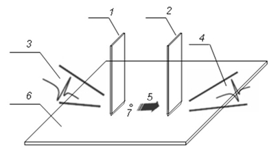
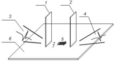
[0026] The idea of ​​the present invention is to place two parallel blades vertically above the surface of the semiconductor to be tested, and inject an electromagnetic wave with a frequency lower than the plasma frequency of the semiconductor into the gap between the cutting edge of one of the blades and the semiconductor, thereby generating surface plasma on the semiconductor surface between the two blades The body wave moves the relative position of the semiconductor and the blade horizontally. When the surface plasmon wave passes through the defects on the surface or inside of the semiconductor, the electromagnetic wave signal emitted from the gap between the edge of the other blade and the semiconductor, and the surface plasmon wave in the semiconductor The defect on the surface that passes the same distance but does not exist on the surface or insi...


PUM


Abstract

The invention discloses a semiconductor defect detection method based on surface plasma wave, and is used for detecting the semiconductor surface flatness or the internal defect of a semiconductor film. According to the invention, an electromagnetic wave with frequency lower than the semiconductor plasma frequency enters a slit between the blade edge and the semiconductor to be detected so as to generate a surface plasma wave on the semiconductor surface. The surface plasma wave can be coupled into a space radiation electromagnetic wave at the slit position between another blade edge and the semiconductor to be detected so as to be received by a detector. By changing the relative positions of the blade and the semiconductor in the horizontal direction, when a surface plasma wave passes through the defective position on the surface or inside of the semiconductor to be detected, the outgoing electromagnetic wave signal correspondingly changes so that the semiconductor surface unflatness or the internal defect of the semiconductor can be detected according to the principle. Compared with the prior art, the method disclosed by the invention has the advantages of wide application range, flexibility in use, high detection precision, no damage to detection sample and the like.

Description

technical field [0001] The invention relates to a semiconductor defect detection method, in particular to a semiconductor defect detection method based on surface plasma waves, which is used for detecting the flatness of the semiconductor surface or internal defects of a semiconductor film. Background technique [0002] Semiconductor devices require a high degree of crystal perfection, but even with the most sophisticated technology, perfect semiconductor crystals are not guaranteed to be 100% obtainable. Crystalline defects can cause uneven silicon dioxide film growth, poor deposition of epitaxial films, unevenly doped layers, and other problems that lead to process problems. In the finished device, crystal defects can cause unwanted current leakage, preventing the device from operating at normal voltages. In the semiconductor component industry, people put forward particularly high requirements for accurate and comprehensive detection of specific damage and defects caused...

Claims


Application Information

Patent Timeline
Patent Type & Authority Applications(China)
IPC IPC(8): G01N21/88G01B11/30
Inventor 杨涛何浩培李兴鳌周馨慧黄维
Owner NANJING FANGYUAN GLOBAL DISPLAY TECH
Why Eureka
Try Eureka