Light emitting diode module for line light source

Inactive Publication Date: 2008-01-24
SAMSUNG ELECTRONICS CO LTD
View PDF6 Cites 17 Cited by
  • Summary
  • Abstract
  • Description
  • Claims
  • Application Information

AI Technical Summary

Benefits of technology

[0015]The present invention has been made to solve the foregoing problems of the prior art and therefore an aspect of the present inventi

Problems solved by technology

However, the LED module with the above structure is not effective in radiating heat from the LED chip due to the low heat radiation capacity of the MCPCB, and when the heat remains in the package without being radiated, light efficiency is degraded.
In addition, the LED package occu

Method used


Image

  • Light emitting diode module for line light source
  • Light emitting diode module for line light source
  • Light emitting diode module for line light source

Examples


Embodiment Construction

[0026]Exemplary embodiments of the present invention will now be described in detail with reference to the accompanying drawings.

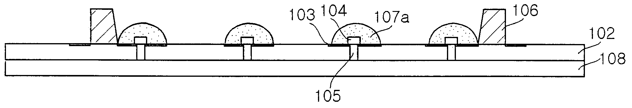
[0027]In the drawings, FIG. 3 is a plan view illustrating an LED module for a line light source according to an embodiment of the present invention, and FIG. 4 is a sectional view illustrating the LED module for a line light source according to an embodiment of the present invention.

[0028]As shown in FIGS. 3 and 4, the LED module 100 for a line light source according to the present invention includes a circuit board 102, a plurality of LED chips 104, a reflecting wall 106 and a heat sink plate 108.

[0029]On the circuit board 102, a wire pattern 103 is formed to supply power and electrical signals to the LED chip 104.

[0030]In addition, vias 105 are formed through the circuit board 102 to assist radiation of the heat from the LED chip 104 to the heat sink plate 108.

[0031]That is, the circuit board 102 has vias 105 formed therethrough to facilitate attachment ...


PUM


Abstract

A light emitting diode module for a line light source includes a circuit board having a wire pattern formed thereon and a plurality of LED chips directly mounted and disposed in a longitudinal direction on the circuit board and electrically connected to the wire pattern. The module also includes a reflecting wall installed on the circuit board to surround the plurality of LED chips, reflecting light from the LED chips. The module further includes a heat sink plate underlying the circuit board to radiate heat generated from the LED chip.

Description

CLAIM OF PRIORITY[0001]This application claims the benefit of Korean Patent Application No. 2006-0069262 filed on Jul. 24, 2006, in the Korean Intellectual Property Office, the disclosure of which is incorporated herein by reference.BACKGROUND OF THE INVENTION[0002]1. Field of the Invention[0003]The present invention relates to a Light Emitting Diode (LED) module for a line light source and, more particularly, to an LED module for a line light source, which increases light emission efficiency and maximizes heat radiation capacity.[0004]2. Description of the Related Art[0005]In general, LED chips are semiconductor devices made of compound materials such as GaAs, AlGaAs, InGaAs, GaN, InGaN, etc. and configured to emit various colors of beams. The LED chips are used in the form of packages, which can be used as light sources for planar displays using liquid crystal displays, etc.[0006]FIG. 1 is a sectional view illustrating a conventional LED module.[0007]Referring to FIG. 1, the conve...

Claims


Application Information

Patent Timeline
IPC IPC(8): H01L29/22H01L33/00F21S2/00F21S8/04F21V8/00F21V29/00F21Y101/02H01L33/44H01L33/48H01L33/50H01L33/54H01L33/56H01L33/60H01L33/64
CPCF21K9/00H01L25/0753H01L33/60H01L33/64H01L2924/0002H01L2924/00
Inventor KIM, IL KU
Owner SAMSUNG ELECTRONICS CO LTD
Why Eureka
Try Eureka