Nonvolatile Memory and Method for Compensating During Programming for Perturbing Charges of Neighboring Cells

a nonvolatile memory and neighboring cell technology, applied in static storage, digital storage, instruments, etc., can solve the problems of reducing the available separation between adjacent states and erroneous reading of stored data, so as to achieve maximum programming performance, reduce the effect of yupin effect and increase performan

Active Publication Date: 2008-01-24
SANDISK TECH LLC
View PDF48 Cites 84 Cited by
  • Summary
  • Abstract
  • Description
  • Claims
  • Application Information

AI Technical Summary

Benefits of technology

[0025] By adjusting the verify level as a function of the target state and the predetermined target memory states of the neighboring memory cells during programming, Yupin effect due to existing or anticipated charges on neighboring cells is compensated for essentially in one programming pass. In practice, the programming may preferably employ more than one phase (e.g., coarse / fine phases) to increase performance, but there is no need to perform two separate passes at completely different times in order to mitigate the Yupin effect. Single-pass programming will allow for maximum programming performance and simpler programming sequence from word line to word line.
[0026] According to another aspect of the invention, the adjusting of the verify level is effected virtually by biasing an adjacent word line accordingly so that when program-verified with the adjusted verify level, the correct target state will be read from the cell in spite of the perturbing charges that are subsequently programmed into neighboring memory cells. This has the advantage of avoiding using a real offset on the verify level of the cell being programmed, thereby avoiding the problem of possibly having the verify level shifted too low to require negative voltage sensing when verifying the lowest memory state.

Problems solved by technology

The coupling from adjacent memory cells can shift the apparent charge level being read a sufficient amount to lead to an erroneous reading of the data stored.
As memory cells continue to shrink in size, the natural programming and erase distributions of threshold voltages are expected to increase due to short channel effects, greater oxide thickness / coupling ratio variations and more channel dopant fluctuations, thereby reducing the available separation between adjacent states.

Method used


Image

  • Nonvolatile Memory and Method for Compensating During Programming for Perturbing Charges of Neighboring Cells
  • Nonvolatile Memory and Method for Compensating During Programming for Perturbing Charges of Neighboring Cells
  • Nonvolatile Memory and Method for Compensating During Programming for Perturbing Charges of Neighboring Cells

Examples


Embodiment Construction

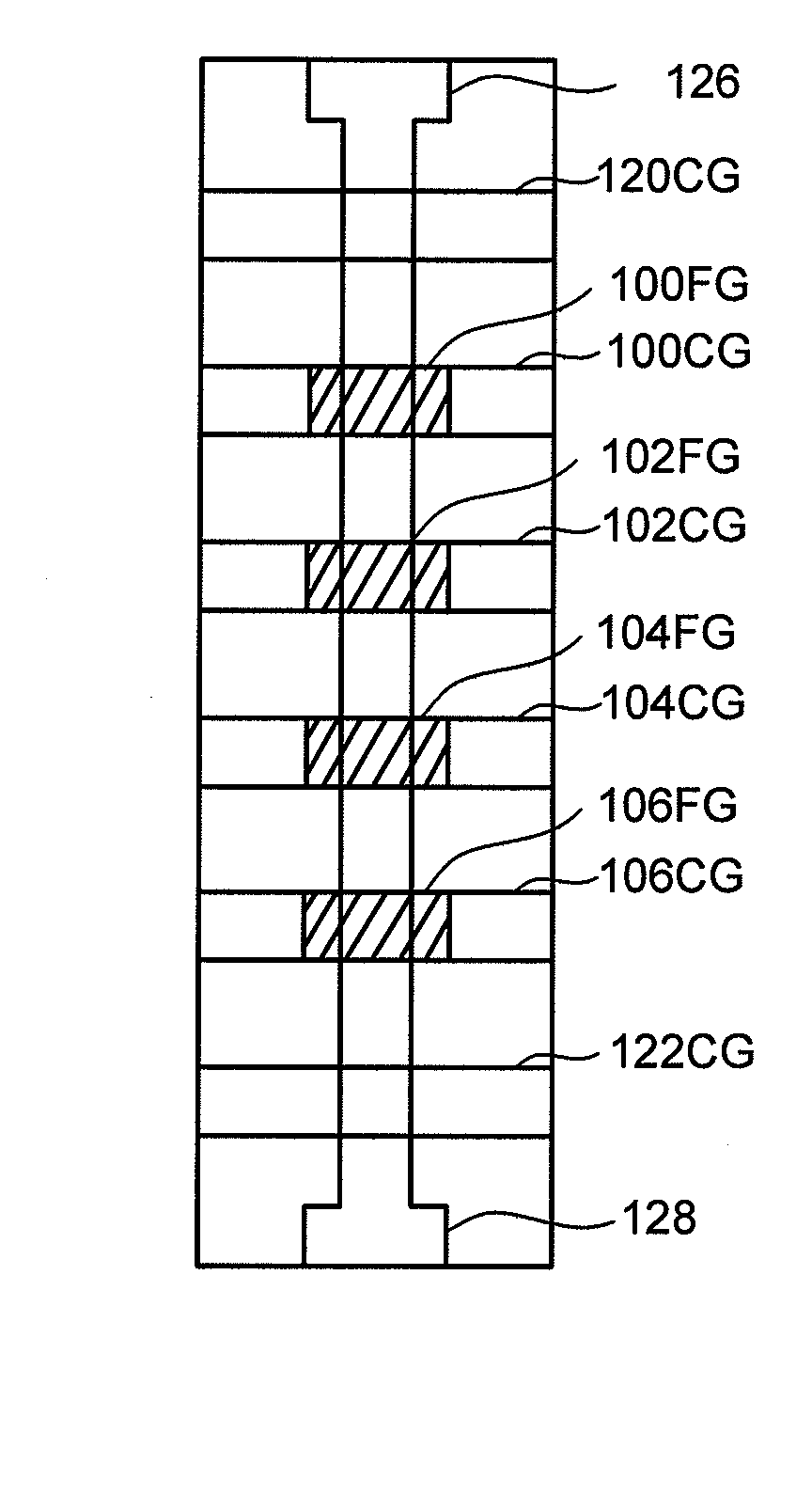
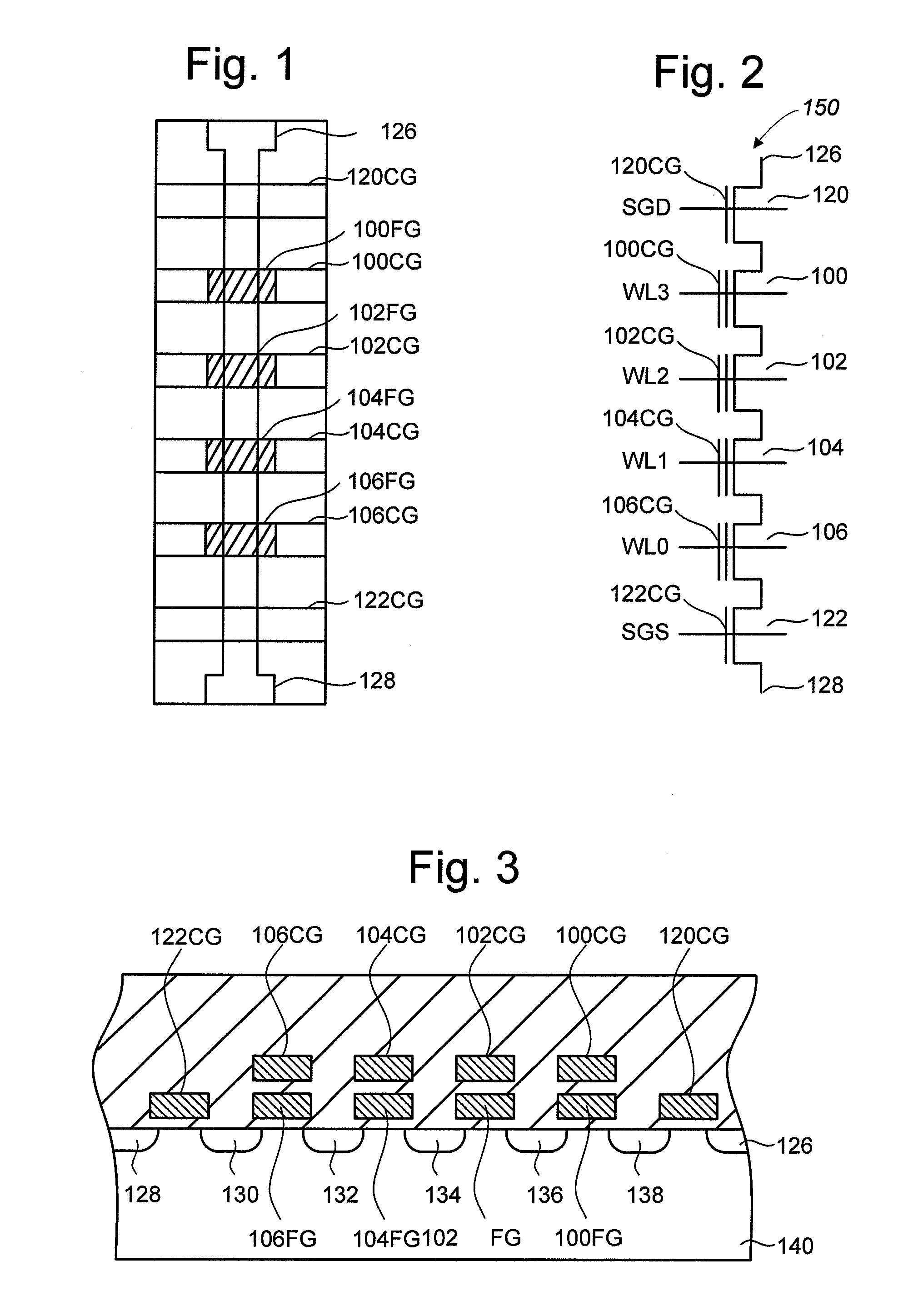
[0078] One example of a memory system suitable for implementing the present invention uses the NAND flash memory structure, which includes arranging multiple transistors in series between two select gates. The transistors in series and the select gates are referred to as a NAND string. FIG. 1 is a top view showing one NAND string. FIG. 2 is an equivalent circuit thereof. The NAND string depicted in FIGS. 1 and 2 includes four transistors, 100, 102, 104 and 106, in series and sandwiched between a first select gate 120 and a second select gate 122. Select gate 120 gates the NAND string connection to bit line 126. Select gate 122 gates the NAND string connection to source line 128. Select gate 120 is controlled by applying the appropriate voltages to control gate 120CG. Select gate 122 is controlled by applying the appropriate voltages to control gate 122CG. Each of the transistors 100, 102, 104 and 106 has a control gate and a floating gate. Transistor 100 has control gate 100CG and f...


PUM


Abstract

Shifts in the apparent charge stored on a charge storing element of a non-volatile memory cell can occur because of the coupling of an electric field based on the charge stored in adjacent charge storing elements. To compensate for this coupling, the programming process for a given memory cell can take into account the target programmed state of one or more adjacent memory cell. The amount of programming is verified after each programming pulse and the standard verify level for the programming cell is dependent on the target state. The verify level is further offset lower dependent on the amount of perturbation from neighboring cells, determinable by their target states. The verify level is preferably virtually offset by biasing adjacent word lines instead of actually offsetting the standard verify level. For soft-programming erased cells, neighboring cells on both adjacent word lines are taken into account.

Description

CROSS-REFERENCE TO RELATED APPLICATIONS [0001] This application is a continuation-in-part of U.S. application Ser. No. 11 / 459,001 filed on Jul. 20, 2006. This application is also related to the following U.S. patent applications which are incorporated by reference herein in their entirety: [0002]“Non-Volatile Memory And Method For Biasing Adjacent Word Line For Verify During Programming,” by Yan Li, Attorney Docket No. 0084567.560US0, filed concurrently herewith, on Sep. 14, 2007. [0003]“Compensating For Coupling Based On Sensing A Neighbor Using Coupling,” by Yan Li and Yupin Fong, Attorney Docket No. SAND-01083US0, U.S. application Ser. No. 11 / 458,997 filed on Jul. 20, 2006; [0004]“System That Compensates For Coupling Based On Sensing A Neighbor Using Coupling,” by Yan Li and Yupin Fong, Attorney Docket No. SAND-01083US1, U.S. application Ser. No. 11 / 459,000 filed on Jul. 20, 2006; [0005]“System That Compensates For Coupling During Programming,” by Yan Li, Attorney Docket No. SAND...

Claims


Application Information

Patent Timeline
Patent Type & Authority Applications(United States)
IPC IPC(8): G11C11/34
CPCG11C8/10G11C16/3454G11C16/3445G11C16/3418
Inventor LI, YAN
Owner SANDISK TECH LLC
Why Eureka
Try Eureka