Silicon microphone and manufacturing method therefor

Inactive Publication Date: 2008-01-24
YAMAHA CORP
View PDF10 Cites 31 Cited by
  • Summary
  • Abstract
  • Description
  • Claims
  • Application Information

AI Technical Summary

Benefits of technology

[0019]According to the aforementioned manufacturing method, it is possible to manufacture the condenser

Problems solved by technology

Variations of stress applied to the conductive layer causes stress to be non-uniformly distributed so that an unwanted deformation or distortion occurs in the diaphragm (and the conductive layer).
This makes electrodes, which are positioned opposite to each other with a prescribed gap therebetween, unexpectedly come in contact with each other in certain areas thereof subjected to relatively large vibration.
Since irregular vibrat

Method used


Image

  • Silicon microphone and manufacturing method therefor
  • Silicon microphone and manufacturing method therefor
  • Silicon microphone and manufacturing method therefor

Examples


first embodiment

1. First Embodiment

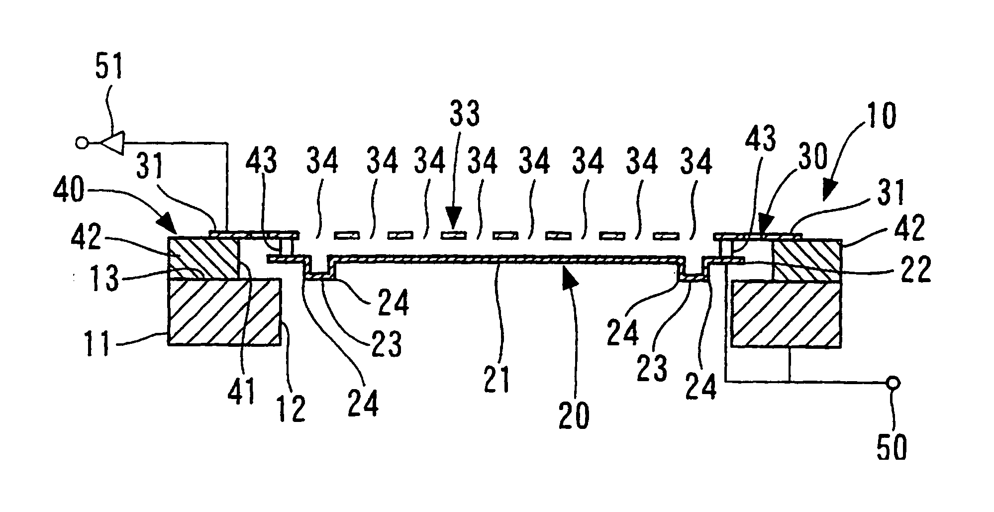
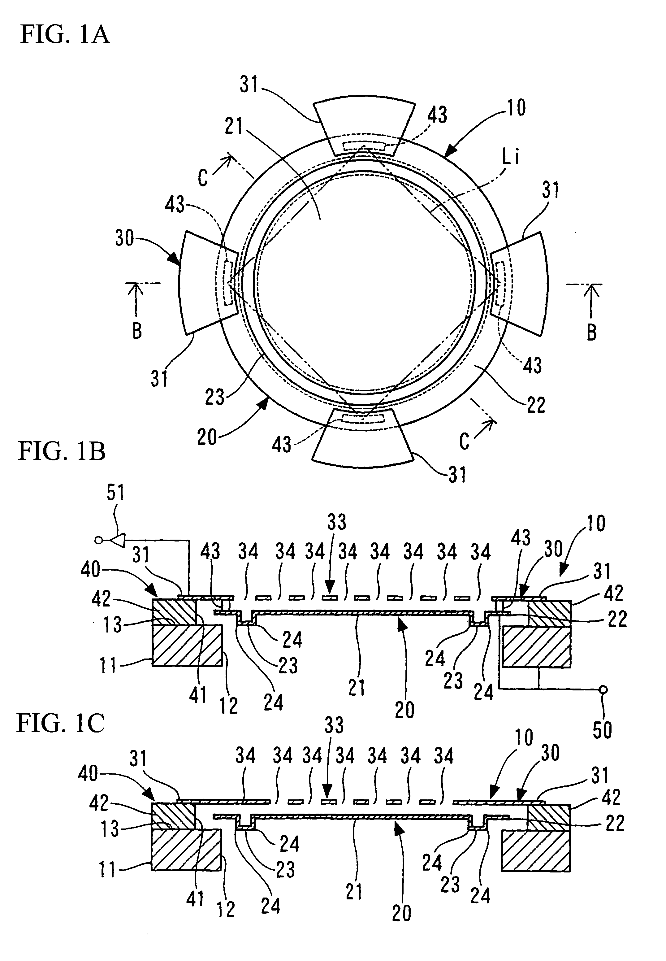
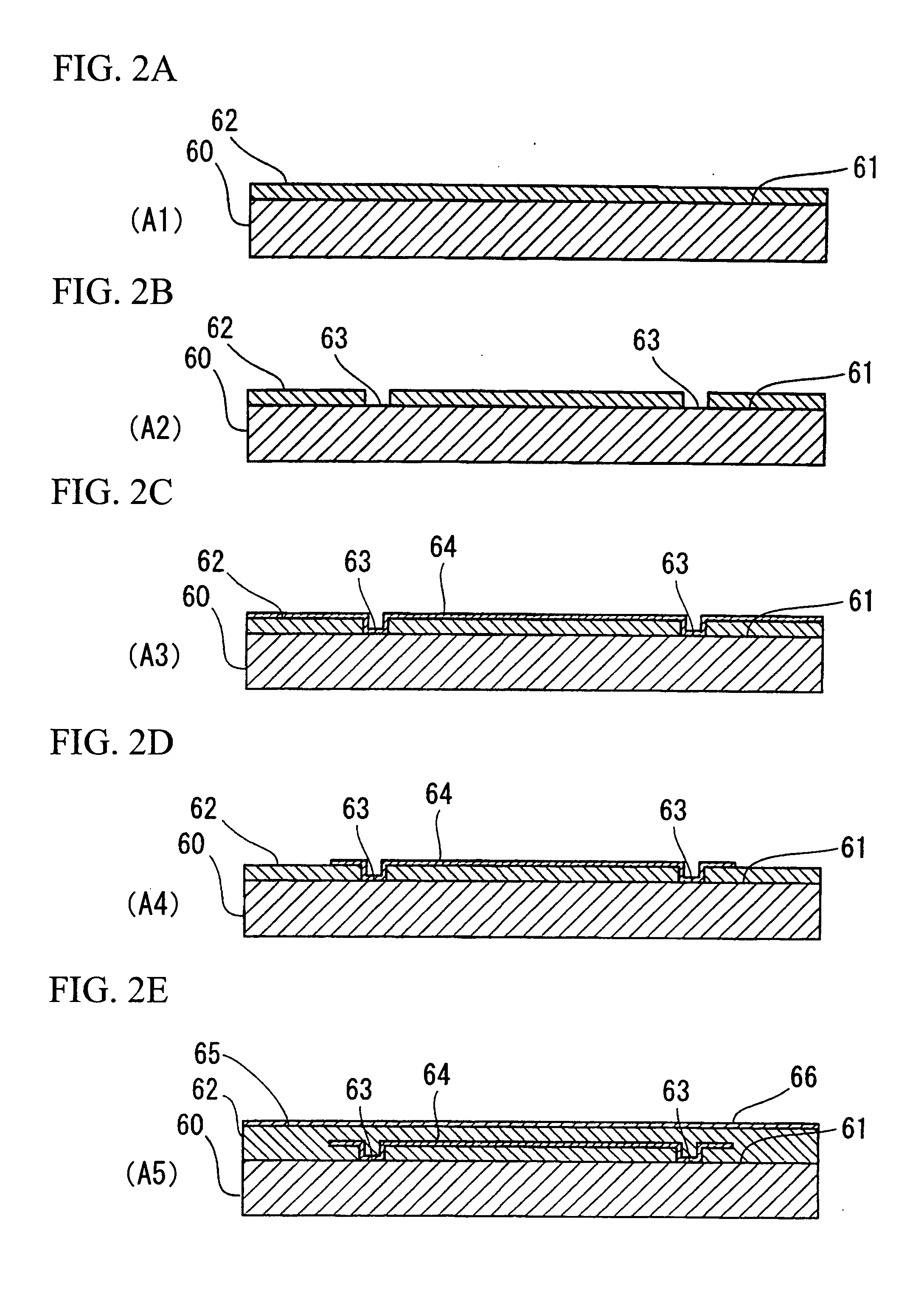
[0073]FIGS. 1A to 1C show a silicon microphone 10 in accordance with a first embodiment of the present invention. The silicon microphone 10 is manufactured by way of the semiconductor manufacturing process.

[0074]The silicon microphone 10 is constituted of a substrate 11, a first conductive layer 20, a second conductive layer 30, and an insulating layer 40. The substrate 11 is composed of monocrystal silicon, for example. The substrate 11 has a cavity 12 realizing an opening therefor. The cavity 12 runs through the substrate 11 in its thickness direction.

[0075]The insulating layer 40 is formed on a surface 13 of the substrate 11. The insulating layer 40 is an oxide layer composed of silicon dioxide, for example. The insulating layer 40 has an opening 41 formed in an interior circumferential portion thereof. The periphery of the opening 41 of the insulating layer 40 forms a support 42 for supporting the second conductive layer 30.

[0076]The second conductive layer 30...

second embodiment

2. Second Embodiment

[0118]With reference to FIGS. 14A and 14B, a condenser microphone 1001 will be described in detail in accordance with a second embodiment of the present invention, wherein the condenser microphone 1001 is a silicon microphone manufactured by way of the semiconductor manufacturing process. The condenser microphone 1001 converts sound waves transmitted via a plate 1030 into electric signals.

[0119]A sensing portion of the condenser microphone 1001 includes a substrate 1010 and first, second, third, and fourth films, which are laminated together.

[0120]The substrate 1010 is composed of monocrystal silicon. The substrate 1010 has a cavity 1011 for releasing pressure that is applied to a diaphragm 1020 in a direction opposite to the propagation direction of sound waves.

[0121]The first film is an insulating thin film composed of silicon dioxide. A first support 1012 is formed by use of the first film so as to support the second film above the substrate 1010 in such a way...


PUM

PropertyMeasurementUnit
Thicknessaaaaaaaaaa
Areaaaaaaaaaaa

Abstract

In a silicon microphone, a corrugation is formed in a conductive layer between a center portion forming a diaphragm and a periphery, wherein the corrugation is formed on an imaginary line connecting a plurality of supports formed in a circumferential direction of the conductive layer, whereby it is possible to increase the rigidity of the conductive layer; hence, distortion or deformation may hardly occur in the conductive layer irrespective of variations of stress applied thereto. Alternatively, a planar portion is continuously formed on both sides of a step portion in the plate so as to increase its rigidity, wherein a plurality of holes are uniformly formed and arranged in the planar portion by avoiding the step portion. Thus, it is possible to realize a high sensitivity and uniformity of performance and characteristics in the silicon microphone.

Description

BACKGROUND OF THE INVENTION[0001]1. Field of the Invention[0002]The present invention relates to silicon microphones and condenser microphones, which are constituted of diaphragms and plates positioned opposite to each other. The present invention also relates to manufacturing methods of silicon microphones and condenser microphones.[0003]This application claims priority on Japanese Patent Application No. 2006-204299 and Japanese Patent Application No.:2006-196586, the contents of which are incorporated herein by reference.[0004]2. Description of the Related Art[0005]Conventionally, various types of silicon microphones and condenser microphones have been manufactured in accordance with manufacturing processes of semiconductor devices. It is well known that silicon microphones are constituted of plates and diaphragms that vibrate due to sound waves. In a conventionally-known example of the silicon microphone, a conductive layer forming a diaphragm is supported by a plurality of suppo...

Claims


Application Information

Patent Timeline
IPC IPC(8): H04R7/06H04R31/00
CPCH04R19/005Y10T29/49005H04R31/00H04R19/04
Inventor SUZUKI, YUKITOSHIHIRADE, SEIJITERADA, TAKAHIRO
Owner YAMAHA CORP
Why Eureka
Try Eureka