Semiconductor device with increased breakdown voltage

a technology of semiconductor devices and breakdown voltages, applied in the field of semiconductor devices with increased breakdown voltage, can solve the problems of reducing the lifetime of the transistor, uncontrollable increase in current, and the breakdown of the transistor, and achieve the effect of not adding additional masking or processing costs

Inactive Publication Date: 2008-01-31
AVAGO TECH INT SALES PTE LTD
View PDF16 Cites 34 Cited by
  • Summary
  • Abstract
  • Description
  • Claims
  • Application Information

AI Technical Summary

Benefits of technology

[0009]The present invention provides a MOSFET device. The MOSFET includes a lightly implanted gate, a heavily implanted drain displaced from the gate, and well regions that begin under a shallow trench isolation region located on opposite sides...

Problems solved by technology

As the operating voltage applied to a transistor increases, the transistor will eventually breakdown allowing an uncontrollable increase in current to pass through the devices.
Operating above the breakd...

Method used


Image

  • Semiconductor device with increased breakdown voltage
  • Semiconductor device with increased breakdown voltage
  • Semiconductor device with increased breakdown voltage

Examples


Embodiment Construction

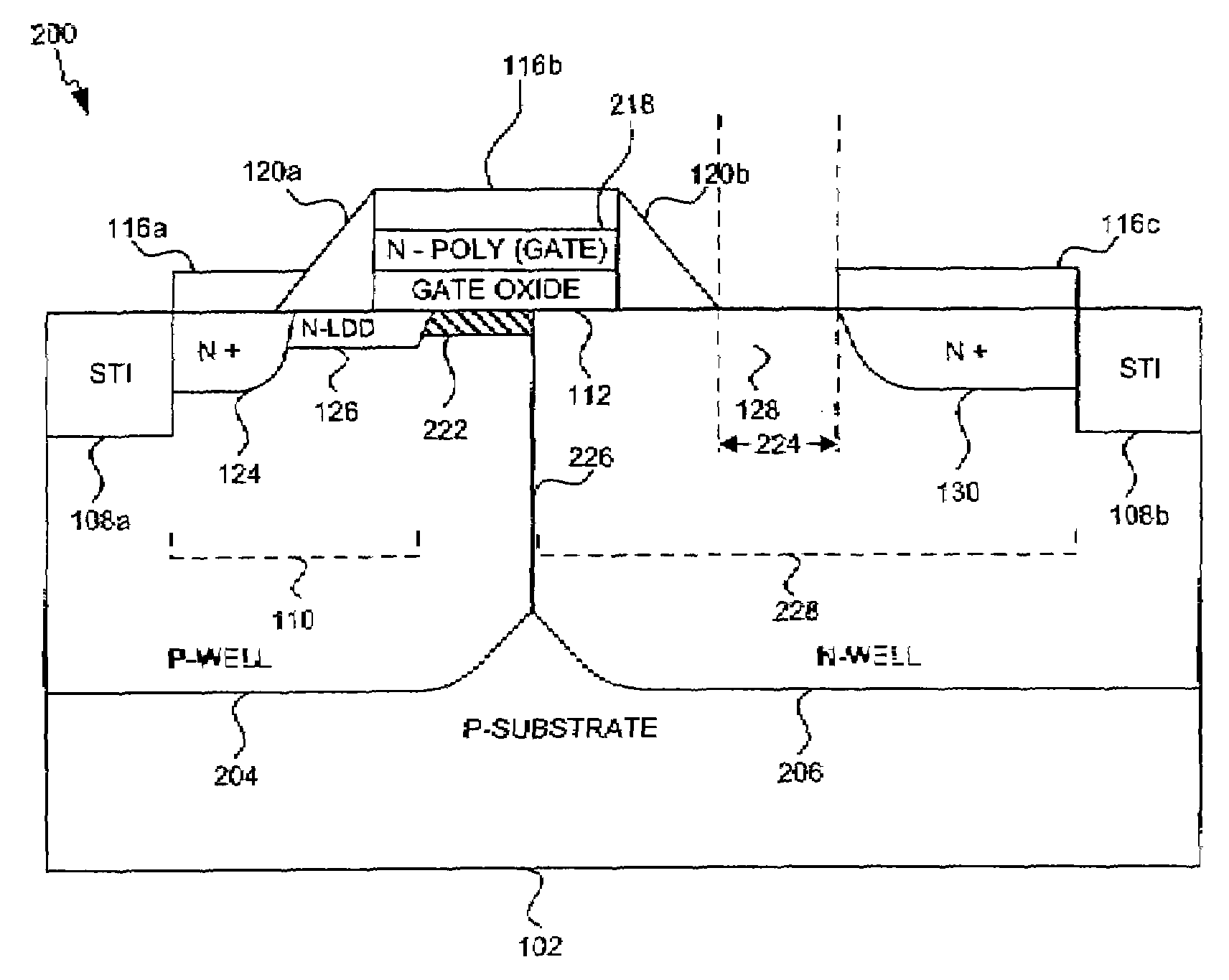
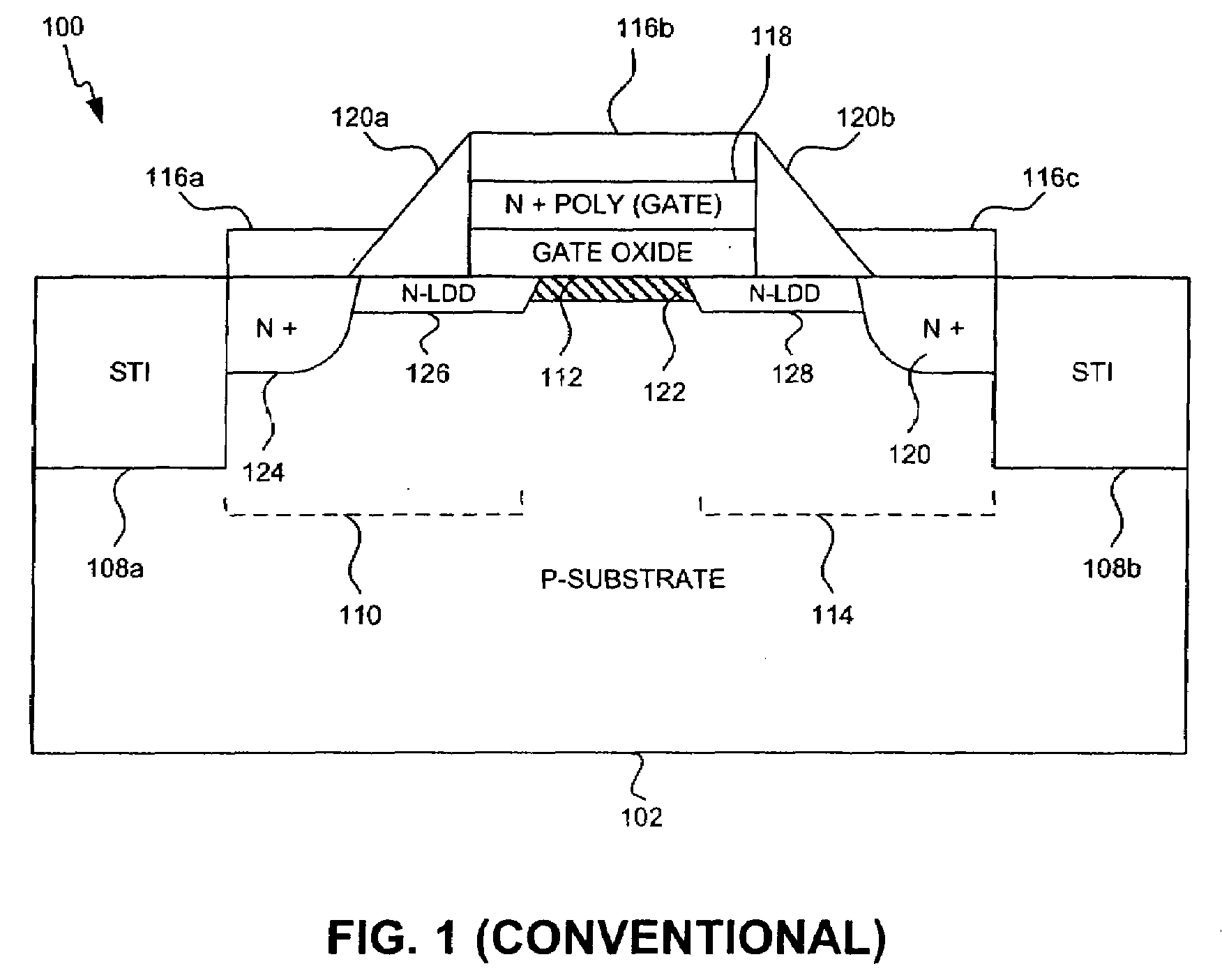
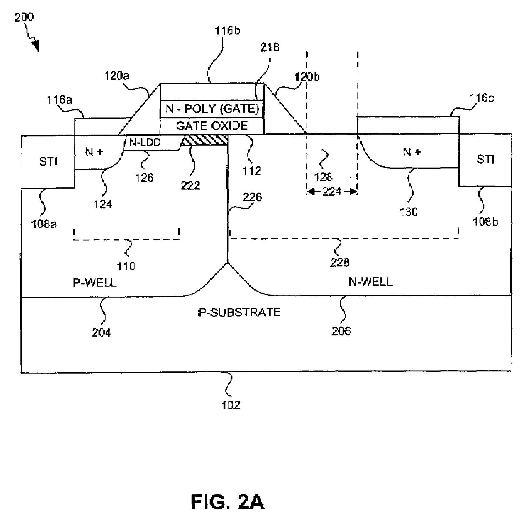
[0017]FIG. 1 illustrates a cross-sectional view of an n-type metal oxide semiconductor (NMOS) structure 100 fabricated using a conventional CMOS logic foundry technology. The conventional CMOS logic foundry technology fabricates NMOS structure 100 onto a p-type substrate 102. Source 110 of NMOS structure 100 includes N+ region 124 and N-LDD region 126. Likewise, drain 114 of NMOS structure 100 includes N+ region 130 and N-LDD region 128. The “+” indicates that the region is implanted with a higher carrier concentration than a region not designated by a “+.” For instance, an N+ region generally has a greater number of excess electrons than an N-type region. A P+ region typically has a greater number of excess holes than the P-type substrate. N-LDD region 126 is in contact with N+ region 124 while N-LDD region 128 is in contact with N+ region 130. N-LDD region 126 and N-LDD region 128 are lightly implanted with n-type material to provide a high resistance shallow diffusion region. N-L...


PUM


Abstract

Optimization of the implantation structure of a metal oxide silicon field effect transistor (MOSFET) device fabricated using conventional complementary metal oxide silicon (CMOS) logic foundry technology to increase the breakdown voltage. The techniques used to optimize the implantation structure involve lightly implanting the gate region, displacing the drain region from the gate region, and implanting P-well and N-Well regions adjacent to one another without an isolation region in between.

Description

CROSS-REFERENCE TO RELATED APPLICATIONS[0001]This patent application claims priority to and is entitled to the benefit of Provisional Patent Application No. 60 / 833,787, filed Jul. 28, 2006, entitled “Semiconductor Device with Increased Breakdown Voltage,” which is incorporated herein by reference in its entirety.BACKGROUND OF THE INVENTION[0002]1. Field of the Invention[0003]The present invention generally relates to semiconductors. More specifically, the invention relates to increasing the breakdown voltage of a semiconductor device.[0004]2. Background Art[0005]Silicon semiconductor processing has evolved sophisticated operations for fabricating integrated circuits. As advancement in fabrication process technology continues, the operating voltage of the integrated circuits has reduced, but the operating voltage of auxiliary devices remains the same. Auxiliary devices are devices used in conjunction with integrated circuits and can include printers, scanners, disk drives, tape drive...

Claims


Application Information

Patent Timeline
IPC IPC(8): H01L29/76
CPCH01L29/0653H01L29/086H01L29/0865H01L29/1083H01L29/7816H01L29/66659H01L29/7835H01L29/1045H01L29/456
Inventor ITO, AKIRACHEN, HENRY KUO-SHUN
Owner AVAGO TECH INT SALES PTE LTD
Why Eureka
Try Eureka