Photodiode and manufacturing method of the same

a photodiode and manufacturing method technology, applied in the field of lateral photodiodes, can solve the problems of natural decrease of the sensitivity of the photodiode, the reduction of the electrode region of the semiconductor, and the reduction of the light receiving efficiency correspondingly, so as to achieve the effect of high sensitivity lateral photodiodes

Inactive Publication Date: 2008-01-31
FUJIFILM CORP
View PDF2 Cites 2 Cited by
  • Summary
  • Abstract
  • Description
  • Claims
  • Application Information

AI Technical Summary

Benefits of technology

[0026]In the mean time, the photodiode manufacturing method according to the present invention includes the steps of: forming protrusions, each having a shape corresponding to each of the microlens, on the semiconductor layer; and stacking the insulat...

Problems solved by technology

The employment of the comb electrode structure in a lateral photodiode, however, causes the semiconductor region to be reduced by the electrode region, and the light receiving efficiency is decreased correspondingly.
The decrease in the light receiv...

Method used


Image

  • Photodiode and manufacturing method of the same
  • Photodiode and manufacturing method of the same
  • Photodiode and manufacturing method of the same

Examples


first embodiment

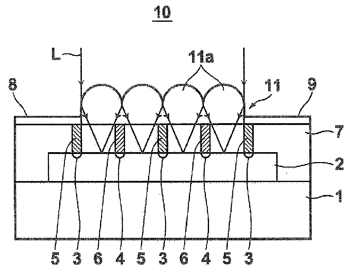
[0040]FIG. 1 is a schematic side view of the lateral photodiode 10 according to the present invention. As illustrated in the drawing, the photodiode 10 includes: a substrate 1; a semiconductor layer 2, formed on the substrate 1, for receiving input light L (detection target light); p-type regions 3 and n-type regions 4 formed parallel to the substrate 1 in the semiconductor layer 2; thin p-type electrodes 5, each connected to each p-type region 3; thin n-type electrodes 4, each connected to each n-type region; a transparent insulation layer 7 formed so as to cover the semiconductor layer from above; an electrode 8 which connects a plurality of p-type electrodes 5; and an electrode 9 which connects a plurality of n-type electrodes 6.

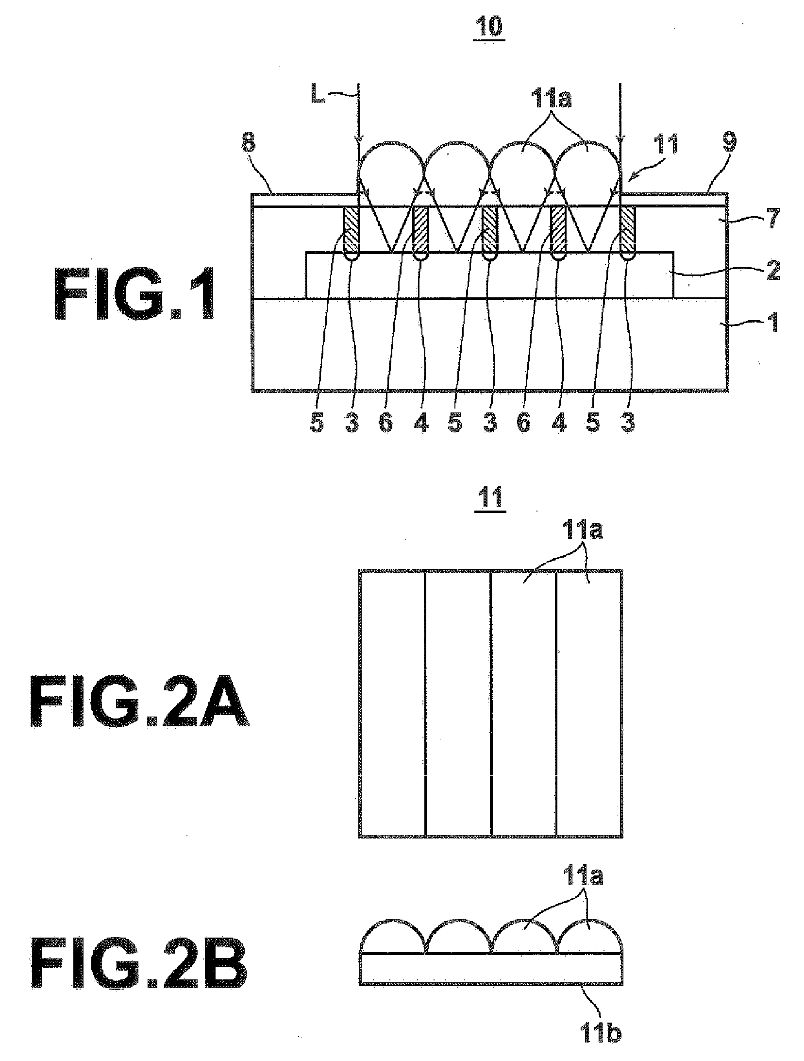
[0041]A microlens array 11 is formed on the insulation layer 7. FIG. 1 illustrates a side cross-section shape of the microlens array 11, and planar shape and side shape are like those illustrated in FIGS. 2A and 2B respectively. That is, the microlens arr...

second embodiment

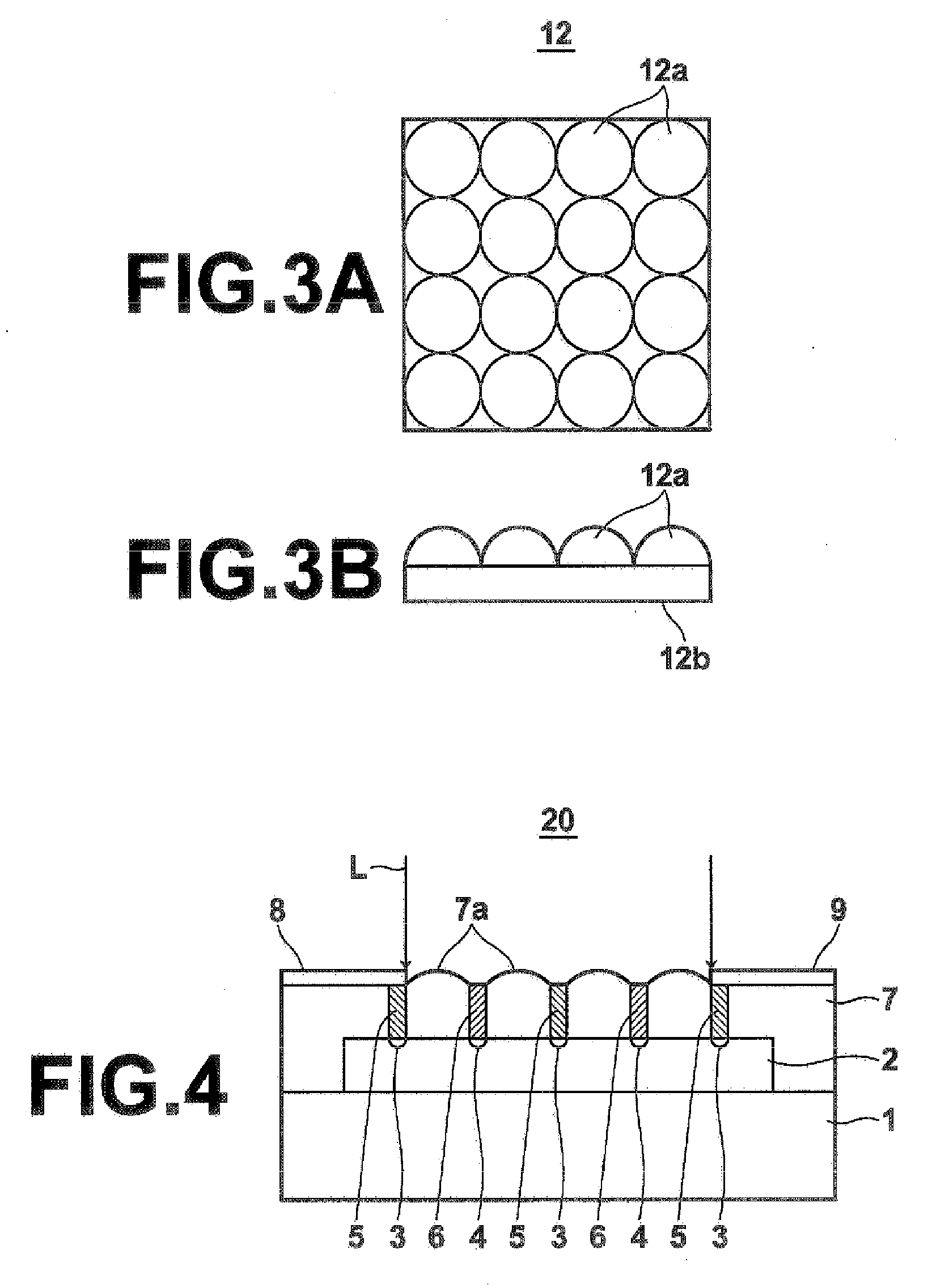
[0046]the present invention will now be described with reference to FIG. 4. In FIG. 4, elements identical to those in FIG. 1 are given the same reference numerals and will not be elaborated upon further here unless otherwise specifically required (the same applies hereinafter).

[0047]In a photodiode 20 according to the second embodiment, a plurality of microlenses 7a is formed on the surface portion of the transparent insulation layer 7. Each of the microlenses 7a is formed in the portion between each of the p-type electrodes 5 and n-type electrodes 6, and focuses the input light L in a manner so as not to be directed to the p-type electrodes 5 and n-type electrodes 6, as in the microlenses 11a in FIG. 1. Therefore, in this case also, the input light L is prevented from being absorbed by the p-type electrodes 5 and n-type electrodes 6, so that the light receiving efficiency is increased and high sensitivity of the lateral photodiode 20 is realized.

[0048]In the present embodiment, the...


PUM


Abstract

A lateral photodiode with increased sensitivity. The lateral photodiode includes: a substrate, a semiconductor layer, formed on the substrate, for receiving input light, an insulation layer formed on the semiconductor layer, and electrodes formed within the insulation layer. A plurality of microlenses is formed over a surface of the insulation layer (or directly on the surface) within a light receiving area of the photodiode, and the input light is focused by the microlenses in a manner so as not to be directed toward the electrodes.

Description

BACKGROUND OF THE INVENTION[0001]1. Field of the Invention[0002]This invention relates to a lateral photodiode and a manufacturing method of the same.[0003]2. Description of the Related Art[0004]Lateral photodiodes, in which a p-type region and an n-type region are arranged parallel to a substrate, are known as described, for example, in Japanese Unexamined Patent Publication No. 5(1993)-175536. FIG. 8 illustrates a basic structure of a lateral photodiode. In the structure, a semiconductor layer 2 for receiving input light L is formed on a substrate 1, and a p-type region 3 and an n-type region 4 are formed parallel to the substrate 1 in the semiconductor layer 2, as illustrated in the drawing. In addition, electrodes 8 and 9 are connected to the p-type region 3 and n-type region respectively, and an insulation layer 7 is formed so as to cover the semiconductor layer from above. In the lateral photodiode structured in the manner as described above, light absorption and carrier movem...

Claims


Application Information

Patent Timeline
IPC IPC(8): H01L31/0232H01L21/00
CPCH01L27/14627Y02E10/50H01L31/03529H01L31/0232H01L31/02327
Inventor INUJIMA, TAKAYOSHIKATO, MIKIHIKO
Owner FUJIFILM CORP
Why Eureka
Try Eureka