High-speed electrical interconnects and method of manufacturing

a technology of high-speed electrical interconnects and manufacturing methods, applied in the direction of waveguides, semiconductor devices, semiconductor/solid-state device details, etc., can solve the problems of increasing the difficulty of high-density interconnects, and increasing the difficulty of interconnecting electronic devices without sacrificing signal speed, etc., to achieve the effect of reducing the effective loss-tangent of the interconnection system material, reducing the effective loss-tangen

Inactive Publication Date: 2008-01-31
BANPIL PHOTONICS
View PDF17 Cites 18 Cited by
  • Summary
  • Abstract
  • Description
  • Claims
  • Application Information

AI Technical Summary

Benefits of technology

[0015] Accordingly, it is an object of the invention to provide a technique to reduce the effective loss-tangent of the interconnec...

Problems solved by technology

Simultaneously achieving higher data rates and higher interconnect densities for both on-chip and also off-chip, will be increasingly difficult as the IC technologies continue to evolve increasing signal speed of electronic devices and interconnection number.
In on-chip cases (inside the die), as the number of the electronic devices such as transistors are increased with continued development of fabrication technology, interconnecting electronic devices without sacrificing signal speed is becoming an increasing challenge.
In the off-chip case, high density interconnects, covering from die-level packaging to chip-to-chip (hereafter chip indicates the die with package) interconnection on the printed circuit board (PCB), will also become increasingly difficult as the IC technologies continue to evolve, thereby increasing the signal speed and interconnection number.
Significant attenuation and rise-time degradation can be caused by losses in the transmission line.
Besides the dissipation-factor of the dielectric materials, the microwave...

Method used


Image

  • High-speed electrical interconnects and method of manufacturing
  • High-speed electrical interconnects and method of manufacturing
  • High-speed electrical interconnects and method of manufacturing

Examples


first embodiment

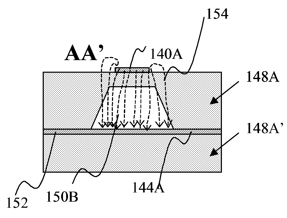
[0131]FIG. 3A is the top view and the FIGS. 3B and 3C are the cross-sectional views of a portion of the interconnects system, taken along AA′ direction of FIG. 3A in the first embodiment in accordance with the invention, wherein the same numerals represents the same parts so that repeated explanation is omitted here. Microstrip line as shown in FIG. 3A is laid onto dielectric system 148, having the opened trenches 150 A (or 150B) into the dielectric system 148 located at the backside of the signal line 140A. The ground plan 152 is located on other dielectric system 148A′. The shape of the opened trenches 150A (and 150B) could be tetrahedral (square, rectangular or circular) or any shaped convenient for manufacturing, and the trenches are filled with the air or any dielectric materials having lower dielectric constant and lower loss tangent. This could be filled with the liquid crystal. By doing this, the refractive index can be tuned based on the electrical field. While signal flowi...

eighth embodiment

[0148] Other combination for placing signal lines on the dielectric system can also be possible. One of the example (not shown) could be the teeth of the upper substrate is front-back (vice-versa) direction, and the signal line is laid along the direction of left right (vice-versa). According to this invention, alternatively, different shape for the dielectric substrate (ground and signal lines) could be thought. One of the examples is the configuration, as shown in FIG. 10, with just opposite to FIG. 9. In FIG. 10, comb-shaped signal substrate 228, sandwiched by the comb-shaped ground substrate 230 (top side) and the thinner ground substrate 232 at the bottom side. In the eighth embodiment, as shown in FIG. 10, the position of the thinner ground plan is located at the bottom and in FIGS. The thinner dielectric substrate is located at the top. Also the teeth direction is downward in FIG. 10, whereas in FIG. 9 the teeth are in upward direction.

[0149] In the preferred embodiment, a po...

eleventh embodiment

[0152] According to this invention, for simplicity, only one microstrip structure with comb-shaped and uniform dielectric substrate are shown in FIG. 12, According to this invention, alternatively, different shape for the dielectric substrate (ground and signal lines) could be thought. One of the examples is the configuration, as shown in FIG. 13, with just opposite to FIG. 12. In the eleventh embodiment, as shown FIG. 13, uniform signal dielectric substrate 250 having the signal line directed towards downward direction, is stacked with comb-shaped dielectric substrate 252 having opening portion is directed in upward direction and the ground plan 144A is in opposite side of the comb-shaped substrate 252. The teethes 254 is in upward direction and the teethes 254 of comb-shaped dielectric substrate 252 directly touch the signal dielectric substrate 250. As explained in FIG. 12, the teeth can be arranged in a direction of front-back (FIG. 13) or left right (vice versa), and the signal...


PUM


Abstract

High-speed interconnect systems for connecting two or more electrical elements for both on-chip and off-chip applications are provided. Interconnect system has the means, which could reduce the microwave loss induced due to the dielectrics. Reducing the effective loss tangent of the dielectrics reduces the microwave loss. With optimize design of the interconnects, the speed of the electrical signal can be made to closer to the speed of the light. The interconnect systems consists of the electrical signal line, inhomogeneous dielectric systems and the ground line, wherein inhomogeneous dielectric system consisting of the opened-trenches into the dielectric substrate or comb-shaped dielectrics to reduce the microwave loss. Alternatively dielectric structure can have the structure based on the fully electronic or electromagnetic crystal or quasi crystal with the line defect. Alternatively, dielectric structure can be made to comb-shaped structure with teethes having thickness and space making the air pocket to reduce the microwave loss. The interconnect system, can be made in rigid or flex board for off-chip interconnects for IC packages, connectors and cables, where conventional manufacturing technology can be used and yet to increase the bandwidth of the interconnects.

Description

PARENT CASE TEXT [0001]“This is a divisional of application(s) Ser. No. 10 / 904,731 filed on Nov. 24, 2004”CROSS REFERENCE TO RELATED APPLICATIONS [0002] This application claims the benefit of U.S. Provisional Patent Application No. 60 / 481 703 filed on Nov. 25, 2003.FIELD OF THE INVENTION [0003] This invention relates to the interconnection of electronics elements in on-chip (inside the chip) and off-chip (board level) level interconnection, high-speed connector, cable fabrication. More particularly, this invention is related to, (a) connecting two or more electronic devices inside the chip, (b) connecting the high speed signal lines two or more chips (e.g. processors), useful in high speed systems including personnel computer (PC) super-computer, game system, imaging system, communication system, and (c) also interface means (as the connector or cable) to connect two or multiple high speed electronics elements. BACKGROUND OF THE INVENTION [0004] The increasing level of integration w...

Claims


Application Information

Patent Timeline
IPC IPC(8): H01L23/52H01L21/4763
CPCH01L23/473H01L23/66H01L25/18H01L2223/6627H01L2924/09701H01L2924/1903H01L2924/3011H01L2924/0002H01P1/2005H01P3/084H01P3/087H01L2924/00
Inventor DUTTA, ACHYUT KUMAR
Owner BANPIL PHOTONICS
Why Eureka
Try Eureka