High Speed Electrical On-Chip Interconnects and Method of Manufacturing

Inactive Publication Date: 2005-05-26
BANPIL PHOTONICS
View PDF0 Cites 26 Cited by
  • Summary
  • Abstract
  • Description
  • Claims
  • Application Information

AI Technical Summary

Benefits of technology

[0015] Accordingly, it is an object of the invention to provide the technique to reduce the effective loss-tangent of the on-chip interconnecti

Problems solved by technology

Simultaneously achieving higher data rates and higher interconnect densities for both on-chip and also off-chip, will be increasingly difficult as the IC technologies continue to evolve with increasing signal speed of electronic devices and interconnection number.
In on-chip cases (inside the die), as the number of the electronic devices such as transistors are increasing with development of the fabrication technology, the interconnecting of the electronic devices without sacrificing the signal speed is getting challenging.
In the on-chip case, high density interconnects, will also be increasingly difficult as the IC technologies continue to evolve with increasing the signal speed and interconnection number.
Significant attenuation and rise-time degradation can be caused by losses in the transmission line.
The repeater usually consists of the active and passive circuits, and each repeater consumes significant power.
Using thousands of repeaters inside the chip requires significant of the power to drive them.
Both metal conductor, traditionally used in on-chip interconnects and also future transmission line (FIG. 3), will have microwave loss, experienced due to the dielectric materials as signal speed incr

Method used


Image

  • High Speed Electrical On-Chip Interconnects and Method of Manufacturing
  • High Speed Electrical On-Chip Interconnects and Method of Manufacturing
  • High Speed Electrical On-Chip Interconnects and Method of Manufacturing

Examples


Embodiment Construction

[0084] The best modes for carrying out the present invention will be described in turn with reference to the accompanying drawings. In the following description, the same reference numerals denote components having substantially the same functions and arrangements, and duplicate explanation will be made only where necessary.

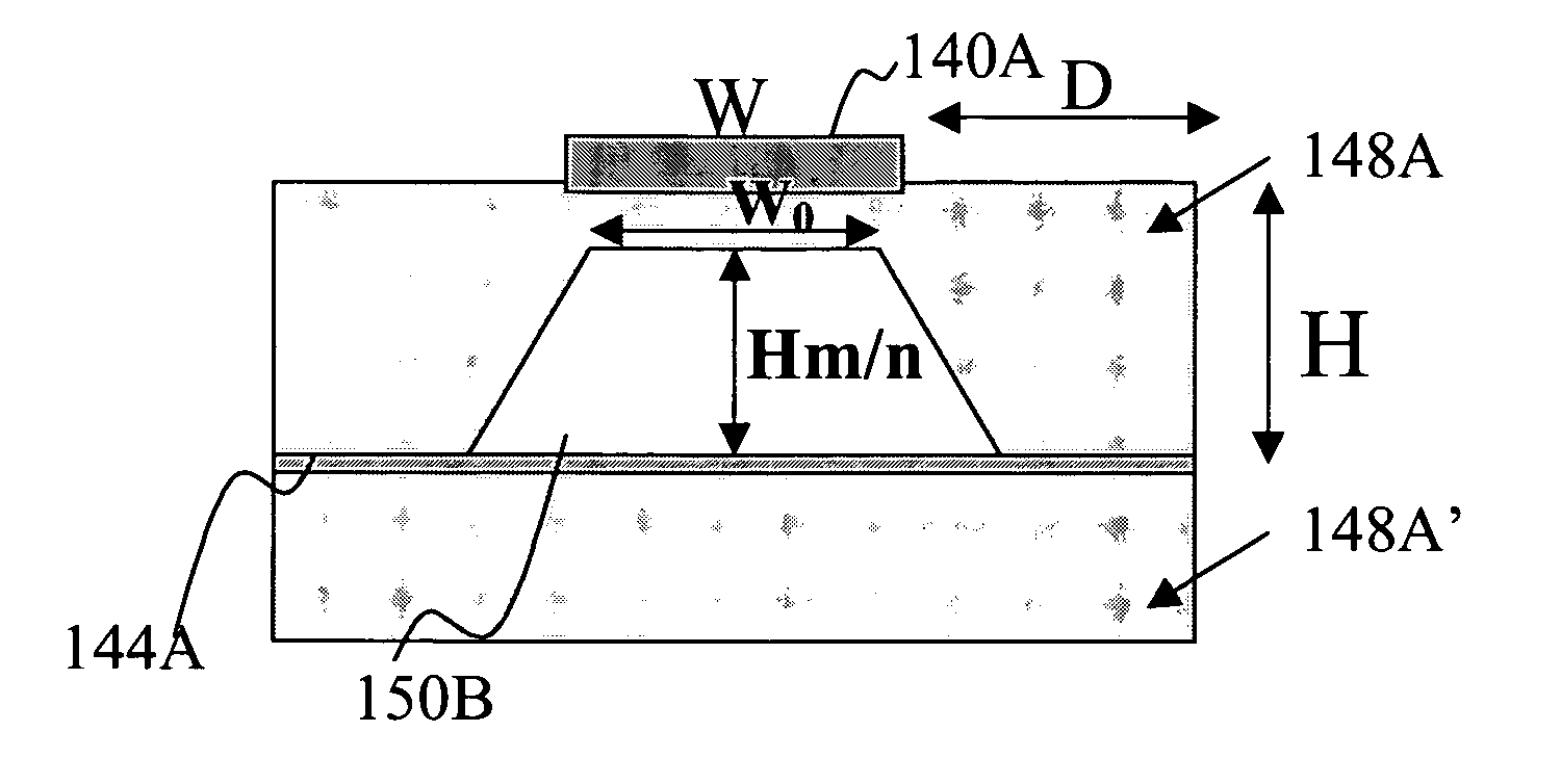
[0085] An important point of high speed electronic interconnects system (for on-chip) according to the invention is that the microwave loss induced due to the dielectrics is to be reduced by reducing the effective loss-tangent of the dielectrics, resulting in increasing the signal carrying capacity of the interconnects. In doing so, the main point is kept into mind that the technique is to be cost effective, and compatible to standard manufacturing technology.

[0086] It is very straight forward that increasing interconnects (on-chip) bandwidth can be possible by using of the low loss-tangent material. However, new materials and related manufacturing technologies...


PUM


Abstract

High-speed interconnect systems for connecting two or more electrical elements are provided for on-chip interconnects. The manufacturing process to fabricate the interconnect structure using standard IC process is also provided. The interconnect systems consists of the electrical signal line, inhomogeneous dielectric systems, and with and without ground line, wherein inhomogeneous dielectric system consisting of the opened-trenches into the dielectric substrate or comb-shaped dielectrics to reduce the microwave loss. The signal lines located below and/or above the opened trenches. The opened trenches helps to reduce the microwave-loss induced due to the dielectric material and increases the on-chip interconnects bandwidth. Alternatively, dielectric system can have the structure based on fully electronic or electromagnetic crystal or quasi crystal with the line defect. The interconnect system, can be made in IC for on-chip interconnects using conventional IC manufacturing technology and yet to increase the interconnects-bandwidth.

Description

CROSS REFERENCE TO RELATED APPLICATIONS [0001] This application claims the benefit of U.S. Provisional Patent Application No. 60 / 481,703 filed on Nov. 25, 2003.FIELD OF THE INVENTION [0002] This invention relates to interconnection of electronics elements in on-chip (inside the chip) interconnection. More particularly, this invention is related to, (a) connecting two or more electronic devices inside a chip by electrical means, useful in high speed chips (processor, memory etc.) for high speed systems including personnel computer (PC) super-computer, game system, imaging system, communication system etc. BACKGROUND OF THE INVENTION [0003] Higher levels of integration within electrical integrated circuits (IC) leads to both higher data rates and larger number of IC interconnections. Today, the inherent signal speed of ICs is around 5 GHz, and shortly it will reach 20 GHz and beyond. The number of pin connection has also increased, with single IC requiring close to 2000 interconnectio...

Claims


Application Information

Patent Timeline
IPC IPC(8): H01L23/498H01L23/66
CPCH01L23/49822H01L23/66H01L2223/6627H01L2924/1903H01L2924/0002H01L2924/3011H01L2924/00
Inventor DUTTA, ACHYUT KUMAR
Owner BANPIL PHOTONICS
Why Eureka
Try Eureka