Stacked ball grid array semiconductor package

a grid array and semiconductor technology, applied in the field of semiconductor packages, can solve the problems of high manufacturing cost, difficult to realize the high integration of semiconductor devices, and many equipment development, and achieve the effect of improving the integration degree and stably stacking

Inactive Publication Date: 2008-01-31
SAMSUNG ELECTRONICS CO LTD
View PDF5 Cites 22 Cited by
  • Summary
  • Abstract
  • Description
  • Claims
  • Application Information

AI Technical Summary

Benefits of technology

[0011]The present invention provides a semiconductor package for improving an integration degree, in which semiconductor packages are stably stacked.

Problems solved by technology

However, for the high integration of the semiconductor chips in the wafer fabrication processes, much research and many equipment developments are needed and fabrication cost also increases.
As a result, it is difficult to realize the high integration of the semiconductor devices.
Therefore, an integration degree of a semiconductor device is limited when the semiconductor packages are stacked according to the conventional art.
Problems with the conventional technologies as described above may obstruct efforts directed to miniaturization and reducing thickness of the stacked semiconductor package.

Method used


Image

  • Stacked ball grid array semiconductor package
  • Stacked ball grid array semiconductor package
  • Stacked ball grid array semiconductor package

Examples


Embodiment Construction

[0020]Preferred embodiments of the present invention will be described below in detail with reference to the accompanying drawings. The present invention may, however, be embodied in different forms and should not be construed as limited to the embodiments set forth herein. Rather, these embodiments are provided so that this disclosure will be thorough and complete, and will fully convey the scope of the present invention to those skilled in the art.

[0021]Also, though terms like a first, a second, and a third are used to describe various regions and materials in various embodiments of the present invention, the regions and the materials are not limited to these terms. These terms are used only to distinguish one region from another region. Therefore, a region referred to as a first region in one embodiment may be referred to as a second region in another embodiment.

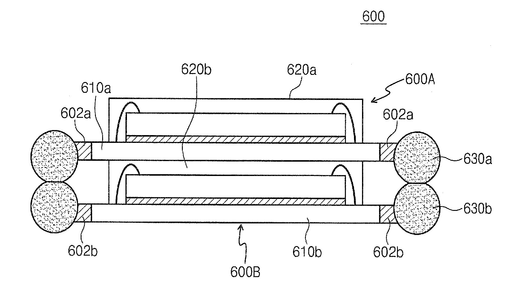
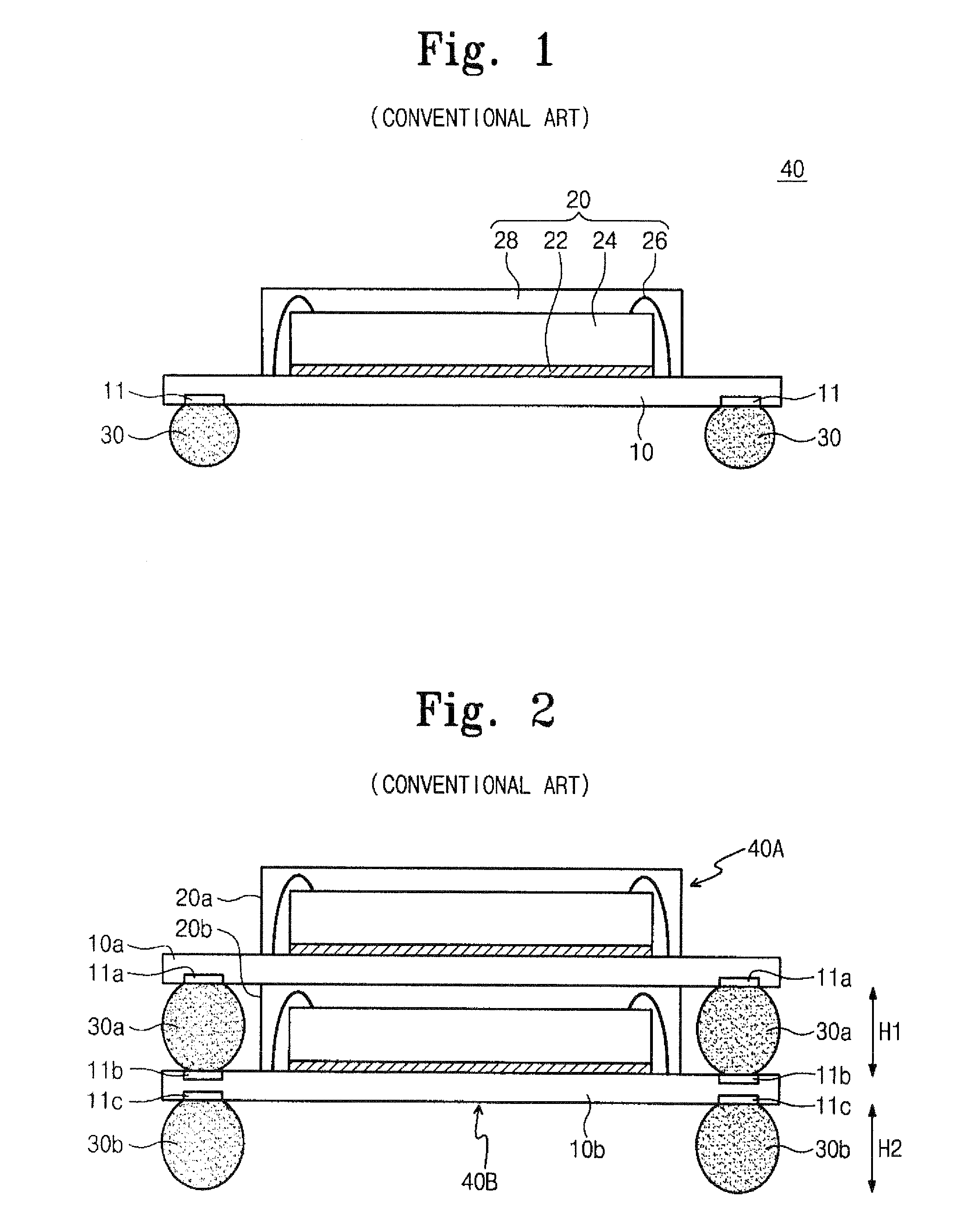
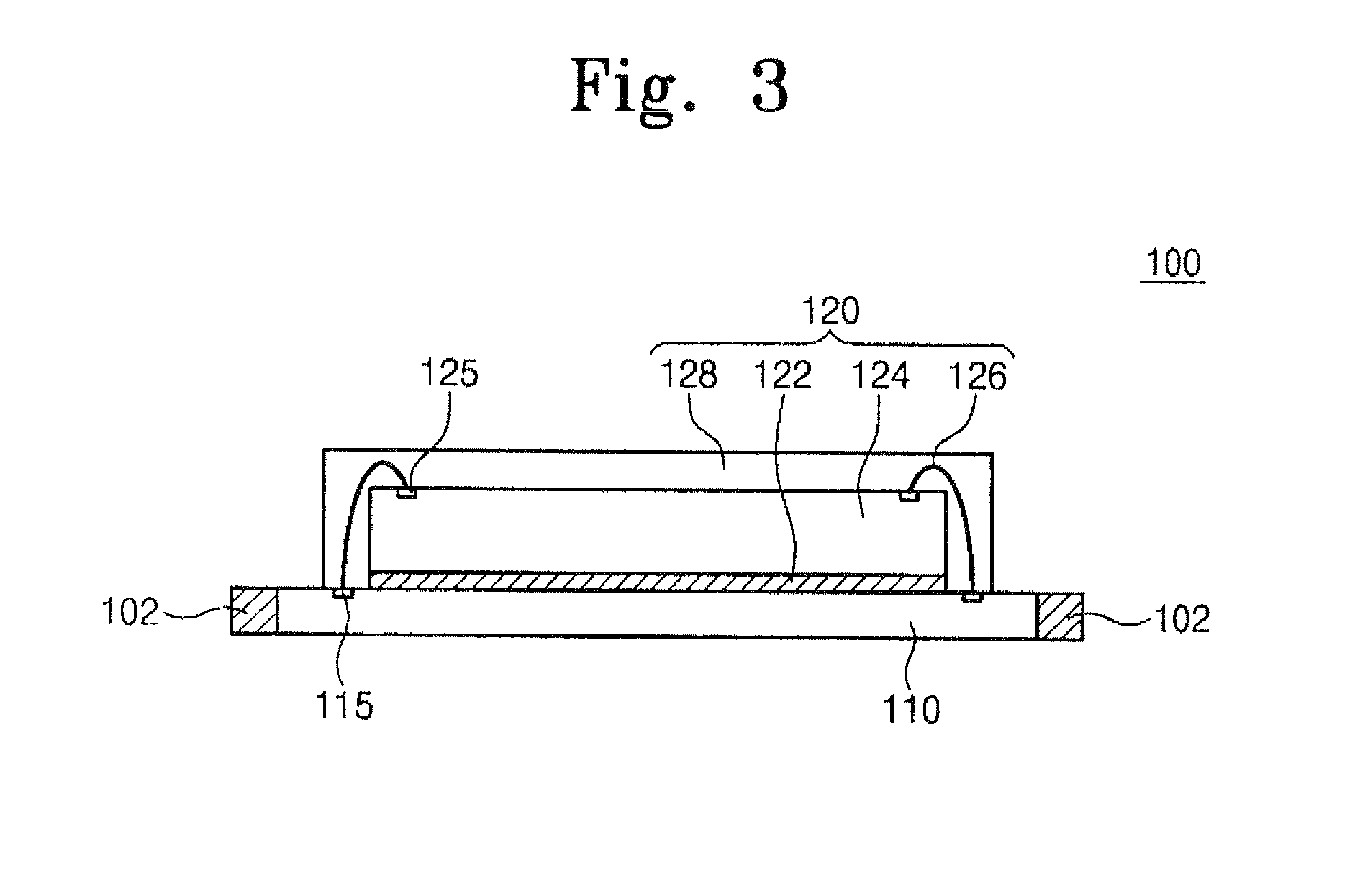
[0022]FIG. 3 is a cross-sectional view of a single semiconductor package according to some embodiments of the present i...


PUM


Abstract

Provided is a stacked ball grid array (BGA) semiconductor package. The stacked BGA semiconductor package includes: a single semiconductor package having landings provided in depressed grooves of both sides thereof, wherein the landings include a conductive material, and a substrate having a semiconductor chip disposed on the substrate; another semiconductor package formed above the single semiconductor package and having landing pads formed in a lower surface of the substrate thereof; and solder balls connecting the landing pads to the landings.

Description

CROSS-REFERENCE TO RELATED APPLICATIONS[0001]This U.S. non-provisional patent application claims priority under 35 U.S.C. § 119 to Korean Patent Application No. 2006-71622, filed on Jul. 28, 2006, the entire contents of which are hereby incorporated by reference.BACKGROUND[0002]1. Technical Field[0003]The present invention disclosed herein relates to a semiconductor package, and more particularly, to a stacked ball grid array (BGA) semiconductor package.[0004]2. Description of the Related Art[0005]Electronic appliances are being developed with the focus on miniaturization, reduced weight, and high speed performance. This has driven many changes in semiconductor device manufacturing in order to keep up with the technological developments of the electronic appliances. Conventional wafer fabrication processes have focused on high integration of semiconductor chips so as to further the miniaturization of the semiconductor devices. However, for the high integration of the semiconductor c...

Claims


Application Information

Patent Timeline
Patent Type & Authority Applications(United States)
IPC IPC(8): H01L23/488
CPCH01L23/49805H01L2924/3511H01L25/105H01L2224/32225H01L2224/48091H01L2224/48227H01L2224/73265H01L2224/83101H01L2224/8385H01L2924/01079H01L2924/15311H01L2924/15331H01L2924/3025H05K3/3442H05K3/368H05K3/403H05K2201/09181H05K2201/09845H05K2201/10515H05K2201/10727H05K2203/041H01L24/48H01L2924/01029H01L2225/1058H01L2225/1023H01L2225/1088H01L24/83H01L2924/00014H01L2924/00H01L2924/00012H01L24/73H01L2924/181Y02P70/50H01L2224/45099H01L2224/45015H01L2924/207H01L23/12
Inventor YANG, SEUNG-YEOL
Owner SAMSUNG ELECTRONICS CO LTD
Why Eureka
Try Eureka