Imprint device and imprint method
a technology of imprint device and imprinting device, which is applied in the field of imprint device and imprint method, can solve the problems of increasing the initial cost of exposure equipment, the insufficient amount of arf laser lithography used in microfabrication, and the sharp rise in the price of masks to achieve resolution equal or near the wavelength of light used in microfabrication
- Summary
- Abstract
- Description
- Claims
- Application Information
AI Technical Summary
Problems solved by technology
Method used
Image

Examples
example 1
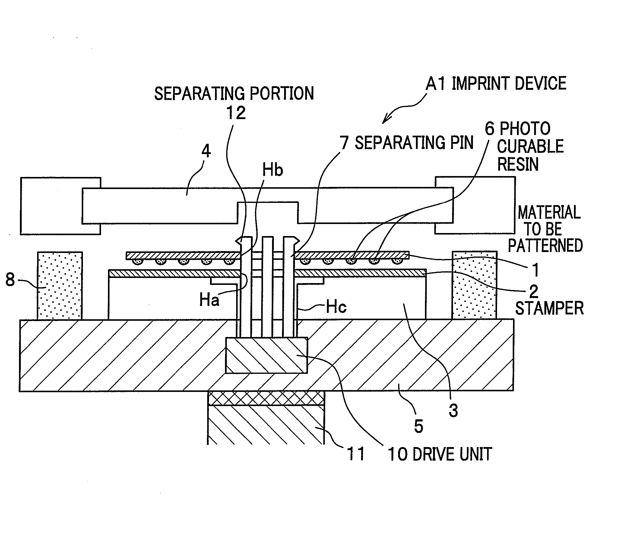
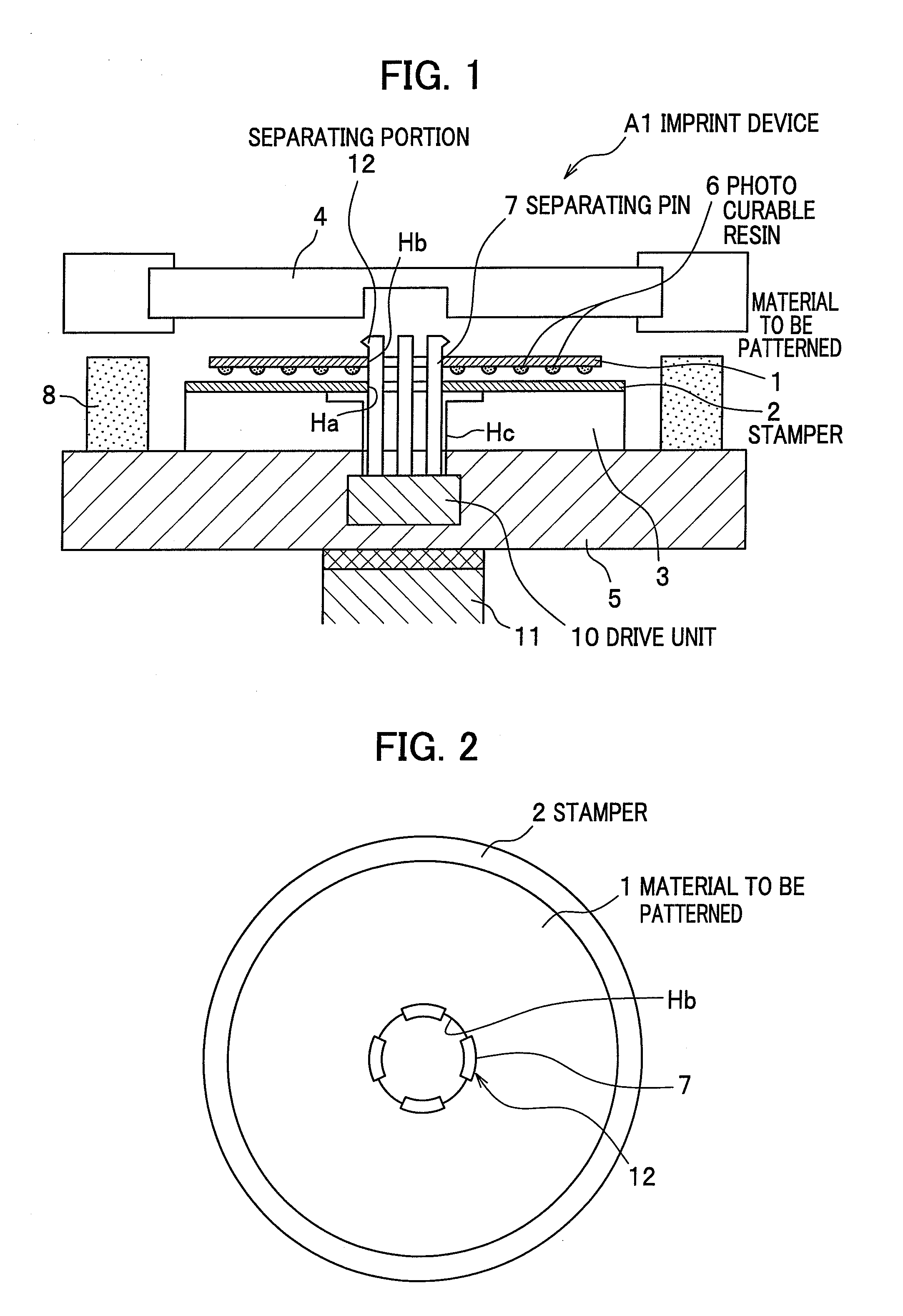
[0068] In Example 1, there was provided a groove structure on one face of a disk substrate.
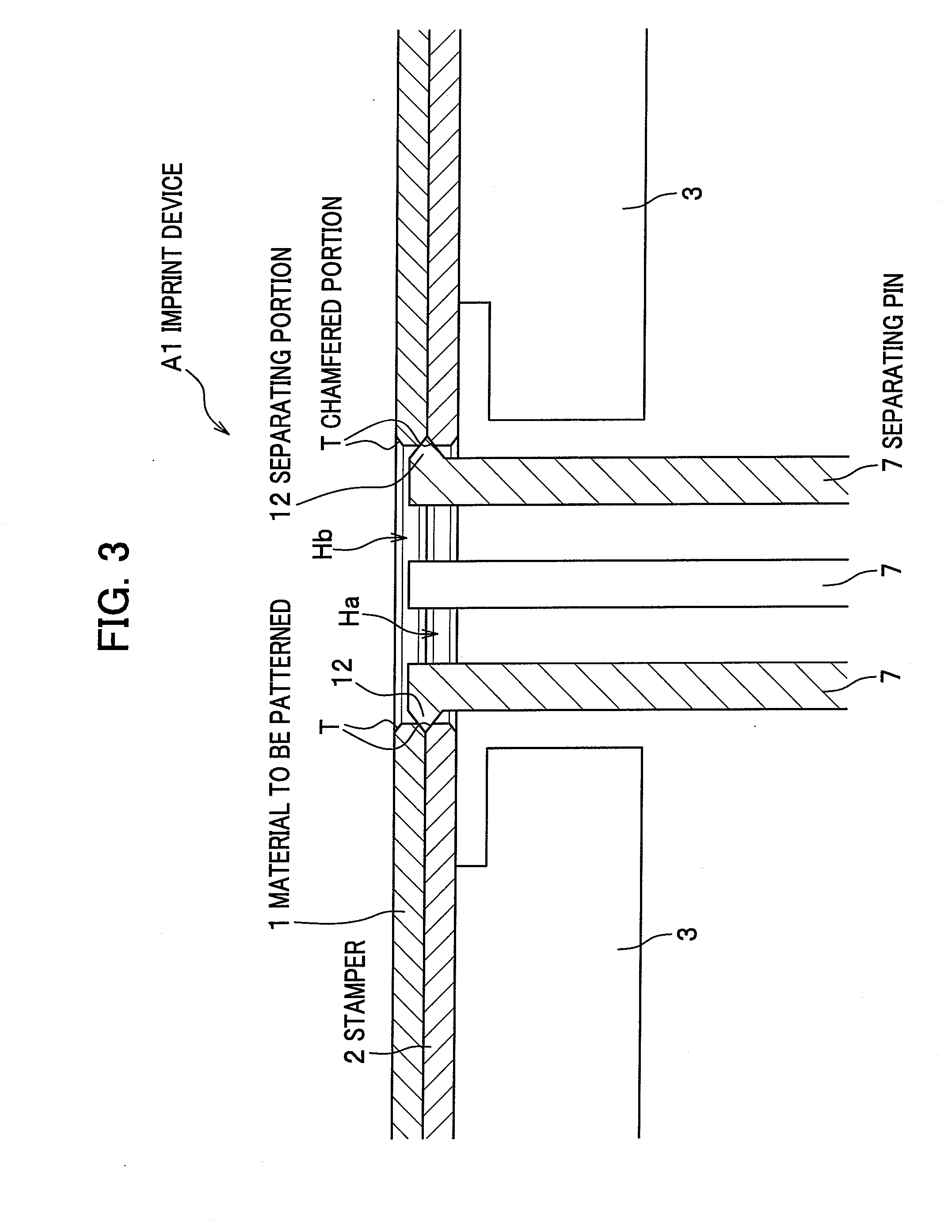
[0069] As for a material to be patterned 1, a glass-disk substrate with a diameter of 65 mm, a thickness of 0.6 mm and a through hole Hb diameter of 20 mm was used. The material to be patterned 1 was prepared such that an end of an outer circumferential thereof and an end of a through hole thereof were chamfered by a width of 0.15 mm, respectively. There was previously provided an acrylate photo curable resin 6 on a face of the material to be patterned 1 in a dispensing method.
[0070] As for a stamper 2, a quartz substrate having the same shape as the above-mentioned material to be patterned 1 was used. On a face of the stamper 2 opposing the material to be patterned 1, there were provided a plurality of concentric grooves in a conventional EB (electron beam direct writing) method. Each of the grooves had a width of 50 nm, a depth of 100 nm and a pitch of 100 nm. The central axis of the groov...
example 2
[0075] In Example 2, there were provided a column structure on both faces of a disk substrate.
[0076] As for a material to be patterned 1, a glass-disk substrate same as that used in the Example 1 was used.
[0077] As for a stamper 2, a pair of quartz substrates having the same shape as the material to be patterned 1 were used. On a face of each of the stampers 2a,2b opposing the material to be patterned 1, there were formed plural pits having a diameter of 0.18 μm, a depth of 0.5 μm and a pitch of 360 nm in a conventional photolithography method, and there was also provided on each of the stampers 2a,2b a ring-like line having a ring-diameter of 62 mm, a width of 0.02 mm, and a depth of 0.5 μm. A center of this ring-like line was arranged to be concentric to the central axis of each of the stampers 2a,2b.
[0078] As shown in FIG. 6A, one stamper 2b (hereinafter referred to as an upper stamper 2b) was fixed to the upper plate 4. The other stamper 2a (hereinafter referred to as a lower...
example 3
[0084] In Example 3, a method for manufacturing a discrete track medium by using the imprint method of the present invention will be described with reference to the drawings if necessary. Of the drawings to be referred to hereinafter, FIG. 9A to FIG. 9D are views for explaining the method of manufacturing the discrete track medium.
[0085] As shown in FIG. 9A, there was prepared a glass substrate 22 obtained in the Example 1, in which there was provided on the glass substrate 22 a pattern formed layer 21 constituted of a photo curable resin 6, on which a surface structure of the stamper 2 had been transferred.
[0086] Next, a surface of the glass substrate 22 was processed in a conventional dry etching method, using the pattern formed layer 21 as a mask. As a result, as shown in FIG. 9B, a structure corresponding to the pattern of the pattern formed layer 21 was etched on the surface of the glass substrate 22. In this example, fluorine-containing gas was used for the dry etching. This...
PUM
| Property | Measurement | Unit |
|---|---|---|
| width | aaaaa | aaaaa |
| width | aaaaa | aaaaa |
| thickness | aaaaa | aaaaa |
Abstract
Description
Claims
Application Information
 - Generate Ideas
- Intellectual Property
- Life Sciences
- Materials
- Tech Scout
- Unparalleled Data Quality
- Higher Quality Content
- 60% Fewer Hallucinations
Browse by: Latest US Patents, China's latest patents, Technical Efficacy Thesaurus, Application Domain, Technology Topic, Popular Technical Reports.
© 2025 PatSnap. All rights reserved.Legal|Privacy policy|Modern Slavery Act Transparency Statement|Sitemap|About US| Contact US: help@patsnap.com