[0008] It is desirable to provide a display device which enables the definition of the display to be high by simplifying the pixel circuit. Particularly, it is desirable to secure sampling
gain of video signals in a simplified pixel circuit.
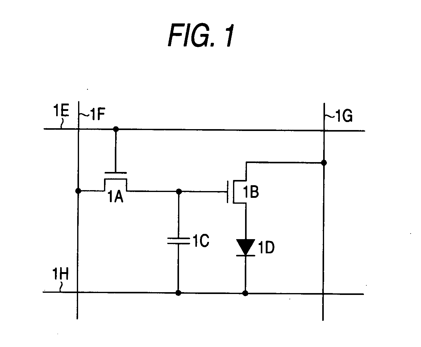
[0010] Specifically, the auxiliary
capacitor is connected to the source of the driving transistor at one end thereof and connected to another power supply line belonging to a previous row from the power supply line of the relevant row at the other end thereof. It is preferable that the main
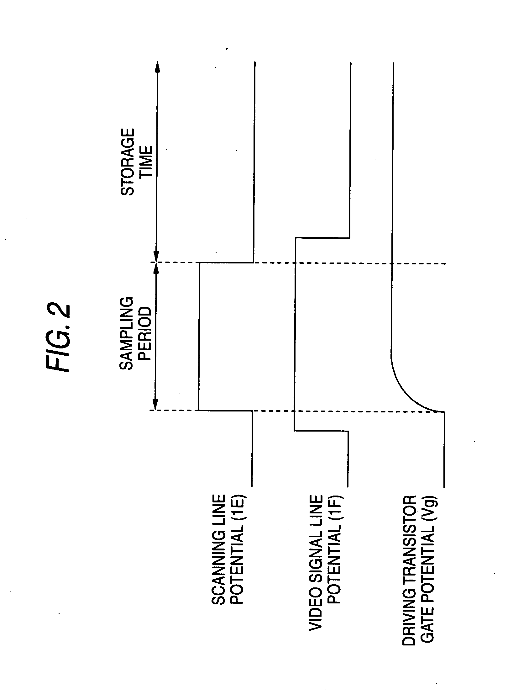
scanner turns off the sampling transistor and electrically disconnects the gate of the driving transistor from the signal line when the signal potential is stored in the storage capacitor, thereby allowing a gate potential to
interlock with variations of a source potential of the driving transistor to maintain a
voltage between the gate and the source to be constant. The main scanner outputs a
control signal for turning on the sampling transistor at a time slot when the power supply line is at the first potential as well as the signal line is at the reference potential to perform a
threshold voltage correction operation for storing a
voltage corresponding to a
threshold voltage of the driving transistor in the storage capacitor.
[0011] The display device according to an embodiment of the invention includes a
threshold voltage correction function, a mobility correction function, a bootstrap function and the like at each pixel. According to the threshold
voltage correction function, threshold voltage variations of the driving transistor can be corrected. In addition, according to the mobility correction function, mobility variation of the driving transistor can be also corrected. According to bootstrap operation of the storage capacitor at the time of emitting light, a regularly
constant light emitting luminance can be maintained, regardless of characteristic variation of the organic EL device. That is, even when current / voltage characteristics of the organic EL device vary with time, a voltage between gate / source of the driving transistor is maintained to be constant by the bootstrapped storage capacitor, therefore, the light emitting luminance can be maintained to be constant.
[0012] According to an embodiment of the invention, the threshold voltage correction function, the mobility correction function, the bootstrap function and the like are incorporated in each pixel, therefore, a
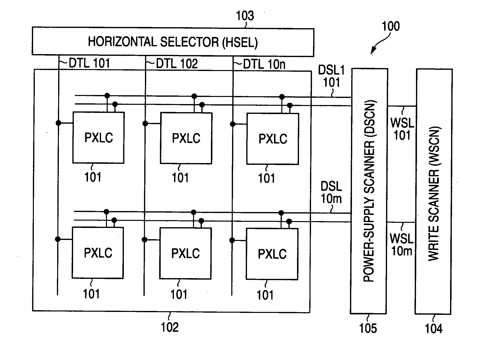
power supply voltage to be supplied to each pixel is used as a switching pulse. By allowing the
power supply voltage to be the switching pulse, a switching transistor for correcting a threshold voltage and a scanning line for controlling the gate are not necessary. As a result, components and wiring of a pixel circuit can be drastically reduced and a pixel area can be reduced, which realizes
high definition of the display. Since the pixel circuit of the related arts which has the above functions have the great number of components, a
layout area becomes large and the circuit is not adequate to the
high definition of the display. However, in the embodiment of the invention, the number of components and the number of wiring are reduced by switching the power supply voltage, as a result, the
layout area of pixels can be reduced.
[0013] As the
fineness of pixels is proceeding, a
capacitance value of the storage capacitor which samples the signal potential of the video signal decreases. Writing
gain of the signal potential is reduced by being affected by wiring
capacitance and
parasitic capacitance. In the embodiment of invention, an auxiliary capacitor is formed in addition to the storage capacitor at each pixel to increase write gain at the time of storing the signal potential in the storage capacitor. In addition, time necessary for correcting mobility can be adjusted by providing the auxiliary capacitor. Accordingly, when driving of the pixel array is performed at high speed, correction of mobility can be sufficiently performed. At that time, one end of the auxiliary capacitor is connected to the source of the driving transistor, and the other end is connected to another power supply line which belongs to a previous row from the power supply line of the relevant row. Accordingly, the threshold voltage correction function of each pixel circuit can be normally performed without receiving potential variations of the power supply line. The auxiliary capacitor is formed between the source and the power supply line of the previous stage, thereby positively performing the threshold voltage correction operation and obtaining the good picture quality.

