

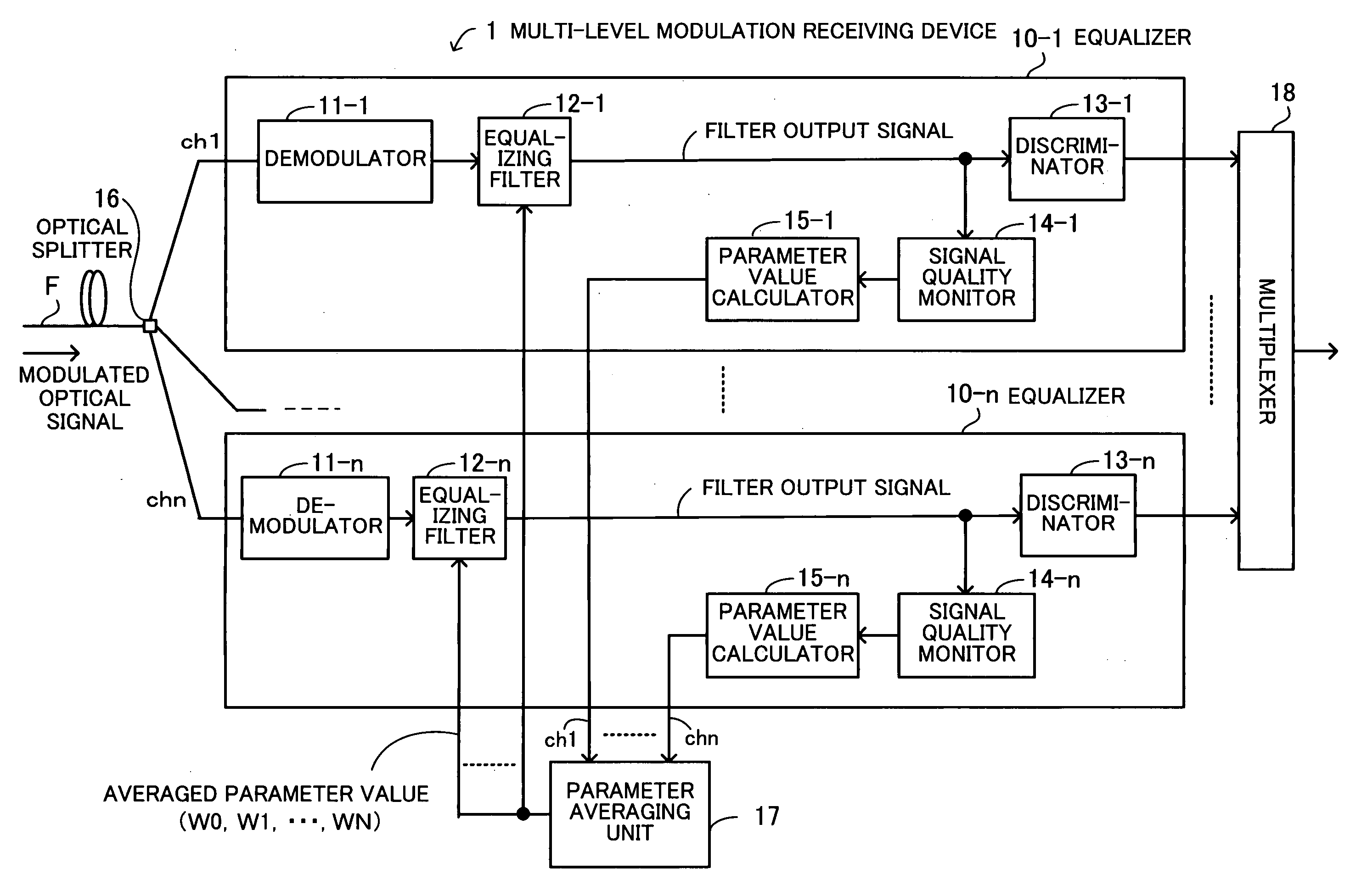
Multi-level modulation receiving device
a receiving device and multi-level technology, applied in electromagnetic receivers, electromagnetic transmission, transmission, etc., can solve the problems of waveform degradation, influence of polarization mode dispersion, and becomes significant, and achieve the effect of short time and high precision
- Summary
- Abstract
- Description
- Claims
- Application Information
AI Technical Summary
Benefits of technology
Problems solved by technology
Method used
Image

Examples
first embodiment
[0108]FIG. 11 shows the configuration of the multi-level modulation receiving device of the first embodiment using the zero-forcing algorithm. A DQPSK optical signal arriving at the multi-level modulation receiving device 1-1 via an optical fiber transmission line F is first split by an optical splitter 16 (1:2 splitter) into two signals, which are supplied to respective receiving circuit channels ch1 and ch2 (corresponding to the equalizers 10-1 and 10-2 in FIG. 1).
[0109]A Mach-Zehnder delay interferometer 11a-1, a differential photodiode 11b-1 and a buffer 11c-1, which are similar to those explained above with reference to FIG. 3, are arranged at the front end of the receiving circuit channel ch1. Also, a Mach-Zehnder delay interferometer 11a-2, a differential photodiode 11b-2 and a buffer 11c-2, which are similar to those explained above with reference to FIG. 3, are arranged at the front end of the receiving circuit channel ch2.
[0110]The Mach-Zehnder delay interferometer 11a-1, ...
second embodiment
[0131]Thus, in the second embodiment, the N variable parameter values p1 to pN are calculated by the variable parameter value calculators CH1 to CHn in such a manner that the variable parameter value calculation process is allotted among the variable parameter value calculators CH1 to CHn.
[0132]FIG. 12 shows the configuration of the multi-level modulation receiving device of the second embodiment. The basic configuration of the multi-level modulation receiving device 1-2 is identical with that of the aforementioned multi-level modulation receiving device 1-1 shown in FIG. 11, and accordingly, operation of the device 1-2 different from that of the device 1-1 will be explained below.
[0133]To calculate the averaged variable parameter value W0, the signal quality index (ch1) and the discriminative signal (ch1) tapped with a delay are multiplied together by the multiplier m11, and the product obtained is input to the averaging integrator b0, thereby obtaining the averaged variable parame...
third embodiment
[0137]FIG. 13 shows the configuration of the multi-level modulation receiving device of the In the multi-level modulation receiving device 1-3 using the least mean square error algorithm, a DQPSK optical signal arriving via an optical fiber transmission line F is first split by an optical splitter 16 (1:2 splitter) into two signals, which are supplied to respective receiving circuit channels ch1 and ch2 (corresponding to the equalizers 10-1 and 10-2 in FIG. 1).
[0138]A Mach-Zehnder delay interferometer 11a-1, a differential photodiode 11b-1 and a buffer 11c-1, which are similar to those explained above with reference to FIG. 3, are arranged at the front end of the receiving circuit channel ch1. Also, a Mach-Zehnder delay interferometer 11a-2, a differential photodiode 11b-2 and a buffer 11c-2, which are similar to those explained above with reference to FIG. 3, are arranged at the front end of the receiving circuit channel ch2.
[0139]The Mach-Zehnder delay interferometer 11a-1, the d...
PUM
 Abstract
Description
Claims
Application Information