Semiconductor Crystal High Resolution Imager

a semiconductor and crystal technology, applied in the field of high-resolution radiation imaging, can solve the problems of high-energy photon emission, limiting factors, and detection sensitivity, and manufacturing is a significant challeng

Active Publication Date: 2008-02-21
RGT UNIV OF CALIFORNIA +1
View PDF15 Cites 52 Cited by
  • Summary
  • Abstract
  • Description
  • Claims
  • Application Information

AI Technical Summary

Problems solved by technology

The radio-label is a positron emitter, which results in high energy photon emissions when positrons annihilate with electrons in body tissue.
Detection sensitivity, though, is another limiting factor.
A difficulty with designs having small scintillation crystals for high resolution is that manufacturing is a significant challenge.
It is costly and complex to handle many minute crystal elements and align them with corresponding photodetector elements.
Slight misalignments might reduce light collection efficiency.
Thus, crystal sheet detectors (e.g. coincidence gamma ray cameras) that have been used in PET suffer from low efficiency for stopping the high energy photons.

Method used


Image

  • Semiconductor Crystal High Resolution Imager
  • Semiconductor Crystal High Resolution Imager
  • Semiconductor Crystal High Resolution Imager

Examples


Embodiment Construction

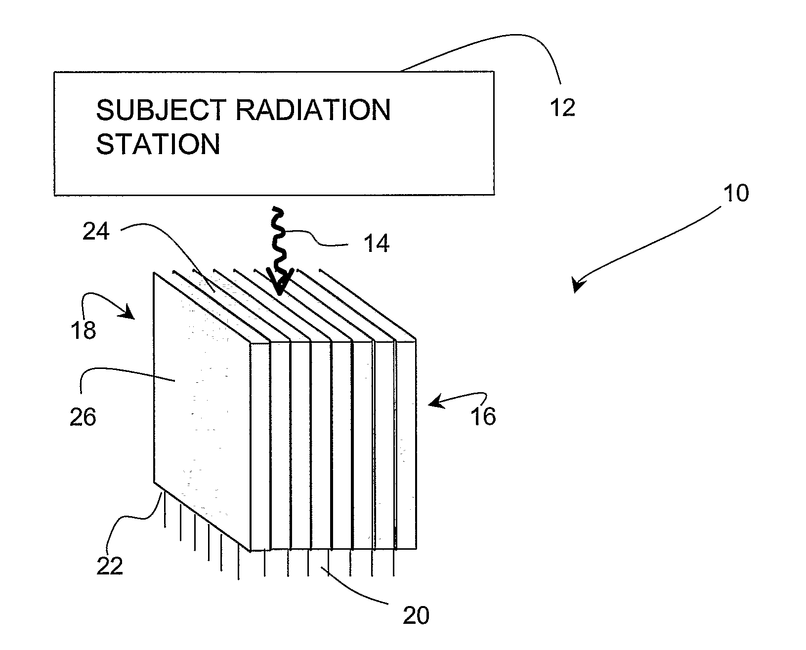
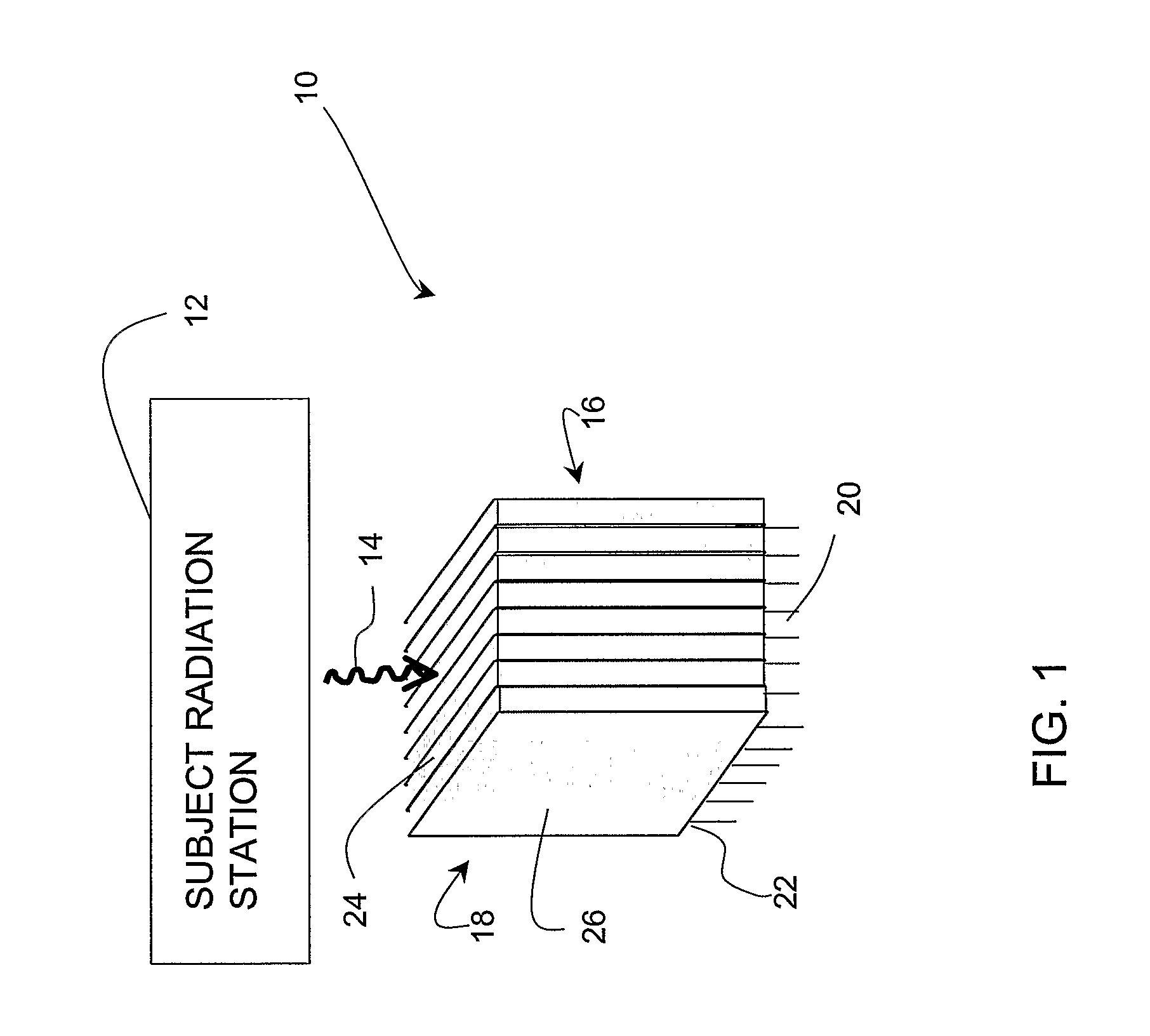
[0035] Preferred embodiments of the present invention provide, among other things, a radiation imaging device that includes a subject radiation station producing photon emissions, and a semiconductor crystal detector that is arranged to directly detect the emitted photons from the radiation station and produce electric pulses. As opposed to conventional radiation imaging such as used in conventional PET, a scintillation crystal is not necessary. This allows direct, and more efficient, conversion of the emitted photons into an electrical signal as compared to scintillation-based detectors.

[0036] The crystal detectors are made from a high-density, high atomic number (z) semiconductor. Such semiconductors are selected from materials that are able to provide the necessary absorption of 511 keV photons for high-quality imaging. In a preferred embodiment, the semiconductor Cadmium-Zinc-Telluride (CZT) is used, though other high-z semiconductors may be used, including but not limited to m...


PUM


Abstract

A radiation imaging device (10). The radiation image device (10) comprises a subject radiation station (12) producing photon emissions (14), and at least one semiconductor crystal detector (16) arranged in an edge-on orientation with respect to the emitted photons (14) to directly receive the emitted photons (14) and produce a signal. The semiconductor crystal detector (16) comprises at least one anode and at least one cathode that produces the signal in response to the emitted photons (14).

Description

PRIORITY CLAIM [0001] This application claims the benefit of U.S. Provisional Application Ser. No. 60 / 614,799, filed Sep. 30, 2004, under 35 U.S.C. §119.TECHNICAL FIELD [0002] A field of the invention is high resolution radiation imaging. An exemplary application of the invention is a positron emission tomography (PET) device. BACKGROUND ART [0003] Scintillation crystals have conventionally been used in non-invasive medical diagnostic techniques that utilize radiation-emitting materials. One such technique is positron emission tomography (PET), which provides in-vivo, functional information about the molecular biochemistry of a given radio-labeled compound (tracer) introduced into a live subject. The radio-label is a positron emitter, which results in high energy photon emissions when positrons annihilate with electrons in body tissue. The tomographic imaging is possible through detection and localization of the many associated highly energetic photons emitted. [0004] In conventiona...

Claims


Application Information

Patent Timeline
Patent Type & Authority Applications(United States)
IPC IPC(8): G01T1/24
CPCH04N5/32
Inventor LEVIN, CRAIG S.
Owner RGT UNIV OF CALIFORNIA
Why Eureka
Try Eureka