Intergrated circuit having memory with resistive memory cells
a resistive memory and intergrated circuit technology, applied in the direction of information storage, static storage, digital storage, etc., can solve the problems of large amount of energy required, reducing the effective electric resistance, and unreliability of evaluation results, so as to improve the method of evaluating the resistive state and improve the resistive memory cell
- Summary
- Abstract
- Description
- Claims
- Application Information
AI Technical Summary
Benefits of technology
Problems solved by technology
Method used
Image

Examples
first embodiment
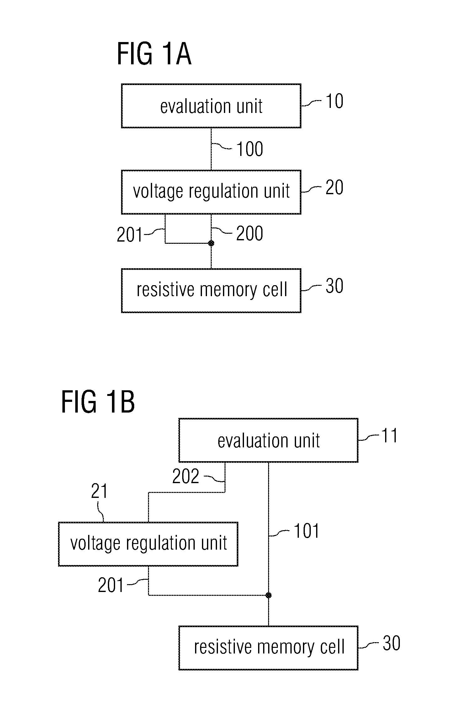
[0024]FIG. 1A shows a schematic view of an evaluation unit 10, a voltage regulation circuit 20, and a resistive memory cell 30, according to the present invention. The resistive memory cell 30 may assume two or more distinguishable resistive states, in this way representing two or more logical states. As an example, a low resistive state may correspond to a logical state “1”, whereas a high resistive state may correspond to a logical state “0”. The resistive memory cell may be based on conductive bridging, phase changing, magnetoresistance, or any other concept for achieving a stable memorization of an electrical resistance. For a reliable distinction between resistive states, the electrical resistance may vary in a sufficient range. In the case of a conductive bridging storage element, variations of the electric resistance by 6 to 7 orders of magnitude may be common. In such a case, a low resistive state may be defined for a resistive memory cell having an effective resistance of a...
second embodiment
[0028]FIG. 1B shows a schematic view of an evaluation unit 11, a voltage regulation circuit 21, and a resistive memory cell 30. According to the present invention, the evaluation circuit 11 applies a sense voltage to the resistive memory cell 30 via a signal line 101. The voltage regulation circuit 21 senses the actually applied voltage at the resistive memory cell 30 via a feedback line 201 and controls the evaluation unit 11 via a control line 202. In this way, the applied voltage is regulated to a target voltage. The evaluation unit 11 may raise the applied voltage to a target voltage.
third embodiment
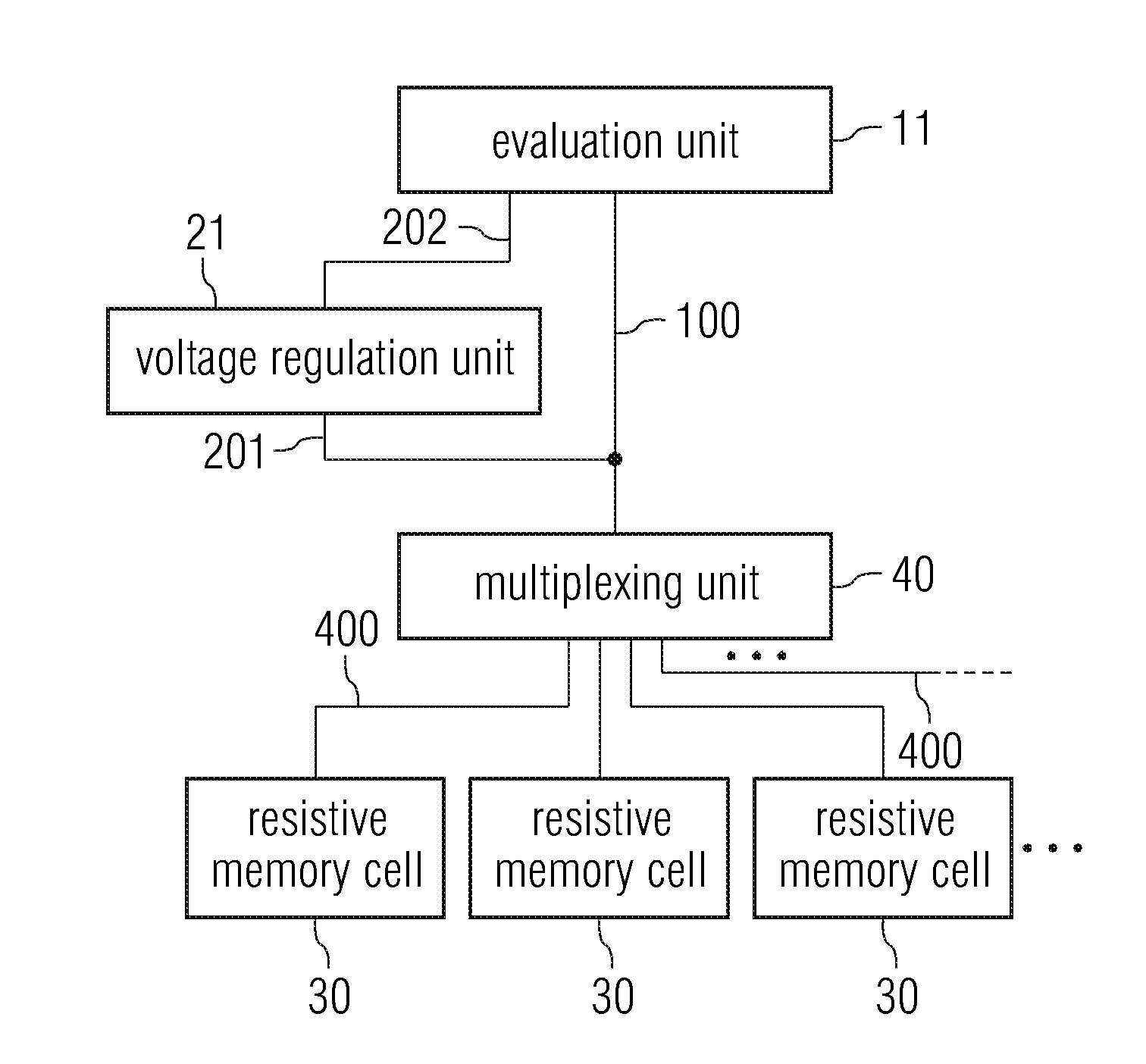
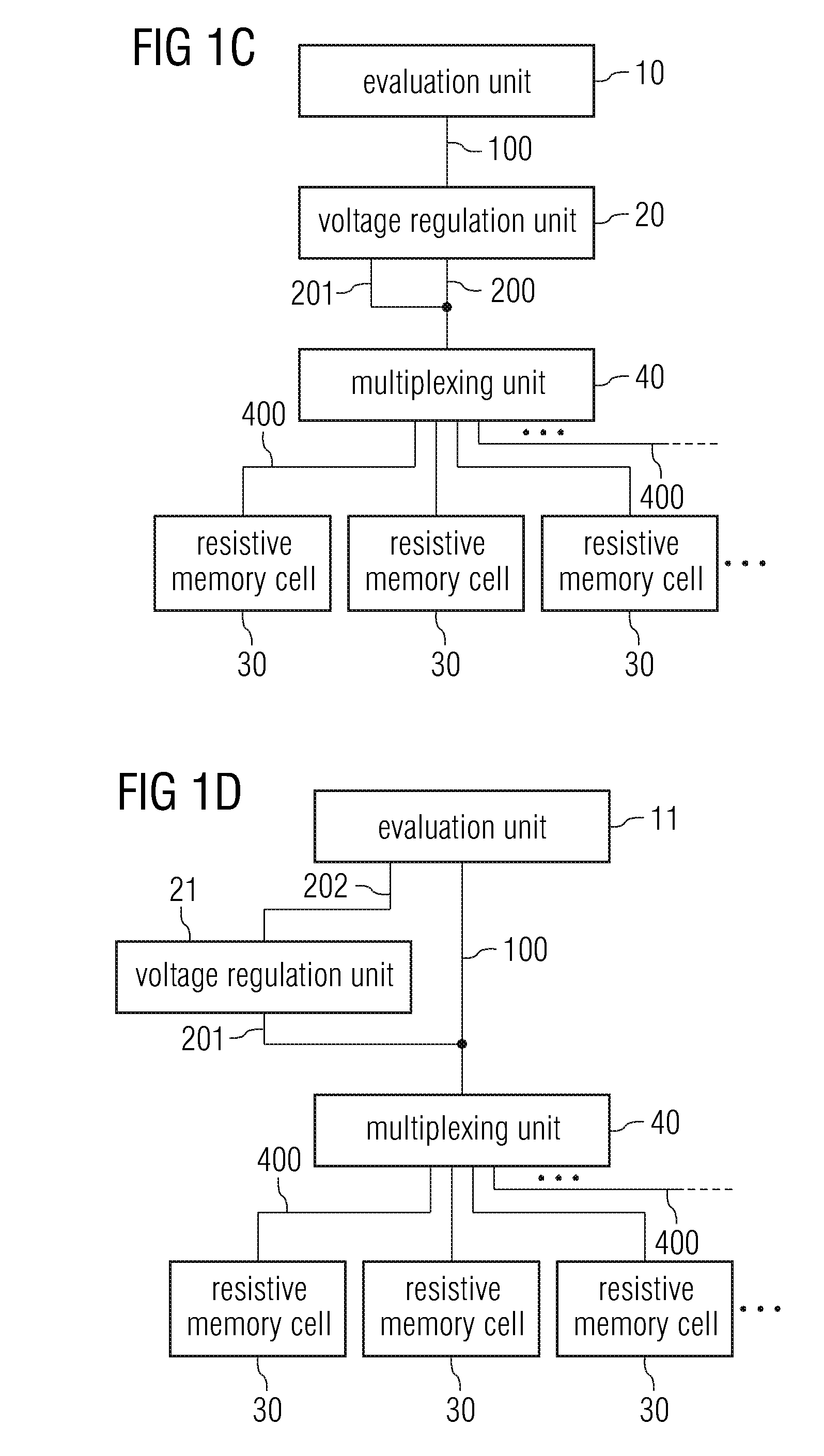
[0029]FIG. 1C shows a schematic view of an evaluation unit 10, a voltage regulation circuit 20, a multiplexing unit 40, and resistive memory cells 30, according to the present invention. According to this embodiment, the master bit line 200 is shared by a plurality of resistive memory cells 30 via the multiplexing unit 40. The bit line 200 then acts as a master bit line. The multiplexing unit 40 connects the master bit line 200 to only one of the bit lines 400 at a time. In this way, the evaluation unit 10 and the voltage regulation circuit 20 may be shared by more than one resistive memory cell 30, which increases device efficiency, performance, and storage capacity.
[0030]FIG. 1D shows a schematic view of an evaluation unit 11, a voltage regulation circuit 21, a multiplexing unit 40, and resistive memory cells 30, representing a combination of the embodiments already described in conjunction with FIGS. 1B and 1C.
PUM
 Abstract
Description
Claims
Application Information
 - Generate Ideas
- Intellectual Property
- Life Sciences
- Materials
- Tech Scout
- Unparalleled Data Quality
- Higher Quality Content
- 60% Fewer Hallucinations
Browse by: Latest US Patents, China's latest patents, Technical Efficacy Thesaurus, Application Domain, Technology Topic, Popular Technical Reports.
© 2025 PatSnap. All rights reserved.Legal|Privacy policy|Modern Slavery Act Transparency Statement|Sitemap|About US| Contact US: help@patsnap.com