

Semiconductor devices the include a fuse part including an antifuse and protection circuit
- Summary
- Abstract
- Description
- Claims
- Application Information
AI Technical Summary
Benefits of technology
Problems solved by technology
Method used
Image

Examples
Embodiment Construction
[0045]An antifuse circuit and a semiconductor memory device that uses the same, according to some embodiments of the present invention, will now be described more fully hereinafter with reference to the accompanying drawings.
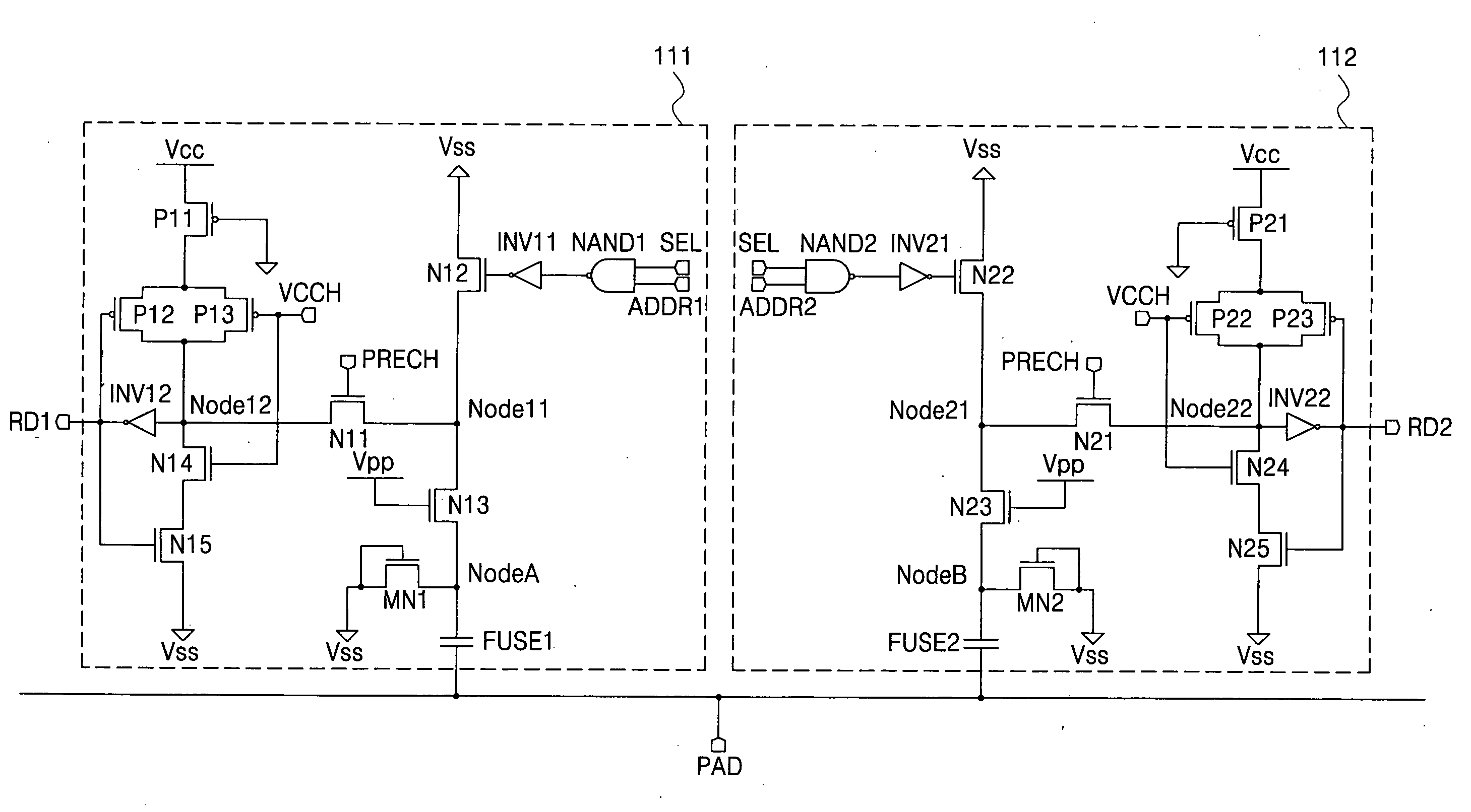
[0046]FIG. 3 is a circuit diagram of an antifuse circuit according to some embodiments of the present invention. Similar to FIG. 2, FIG. 3 illustrates two antifuse circuits 111 and 112 among a plurality of antifuse circuits 10 corresponding to a row or column connected to a pad PAD to which a high voltage Vf is applied from the high voltage generator 30 of FIG. 1.
[0047]In FIG. 3, it is assumed that only a first antifuse FUSE1 of the first antifuse circuit 111 is fused. The antifuse circuits 111 and 112 may have NMOS transistors N11 and N21 that are operable as a switch having one end that may be a fuse part and another end that may be a latch part.
[0048]The NMOS transistors N11 and N21 may switch between their fuse nodes Node11 and Node21 and latch nodes Node12 ...
PUM
 Abstract
Description
Claims
Application Information