Light emitting diode package employing lead terminal with reflecting surface

a technology of light-emitting diodes and lead terminals, which is applied in the direction of discharge tubes/lamp details, discharge tubes luminescnet screens, electric discharge lamps, etc., can solve the problems of deterioration of optical efficiency, low reflectivity, and decrease in the lifespan of led packages, so as to improve the heat dissipation performance of the package, improve the light-emitting efficiency, and reduce the discoloration of the package body

Inactive Publication Date: 2008-02-28
SEOUL SEMICONDUCTOR
View PDF3 Cites 75 Cited by
  • Summary
  • Abstract
  • Description
  • Claims
  • Application Information

AI Technical Summary

Benefits of technology

[0032]According to the present invention, it is possible to provide an LED package employing reflecting surfaces formed by bending parts of lead terminals so that light emitting efficiency can be improved and discoloration of a package body can be reduced. Further, lead terminals having wing portions can be employed to provide reflecting surfaces and to improve the heat dissipation performance of the package. In addition, it is possible to provide an LED package in which a wavelength-converting member with a proper shape can be easily formed by dotting a liquid resin containing phosphor(s).

Problems solved by technology

However, the conventional side-view LED package has a problem in that light emitted from an LED chip toward the inner walls 15w is absorbed and scattered by the inner walls 15w of the package body, which have low reflectivity, resulting in deterioration of optical efficiency.
Thus, as the LED package is used for a long time, the optical efficiency is further deteriorated, resulting in a decrease in the lifespan of the LED package.
Moreover, since the package body 15 made of a material such as PPA has poor heat-dissipating performance, heat generated in the LED chip cannot be easily dissipated to the outside.
As a result, junction temperature increases in the LED chip during operation of the LED chip, leading to deterioration of the optical efficiency.
Meanwhile, if the cavity 16 is filled with the light-transmitting resin 23 containing phosphors, an upper surface of the light-transmitting resin 23 is in the form of a meniscus, resulting in deterioration of the optical efficiency.
If the amount of the light-transmitting resin 23 is increased to solve this problem, the light-transmitting resin 23 protrudes upwardly beyond an upper surface of the package body 15 and thus may be easily damaged by an external force.
However, since the liquid resin flows down due to the flat bottom of the cavity 16, it is difficult to form a convex wavelength-converting member.

Method used


Image

  • Light emitting diode package employing lead terminal with reflecting surface
  • Light emitting diode package employing lead terminal with reflecting surface
  • Light emitting diode package employing lead terminal with reflecting surface

Examples


Embodiment Construction

[0045]Hereinafter, preferred embodiments of the present invention will be described in detail with reference to the accompanying drawings. The following embodiments are provided only for illustrative purposes to fully convey the scope of the present invention to those skilled in the art. Therefore, the present invention is not limited to the embodiments set forth herein but can be implemented in different forms. In the drawings, the widths, lengths, thicknesses and the like of components may be exaggerated for convenience of illustration. Like reference numerals indicate like elements throughout the specification.

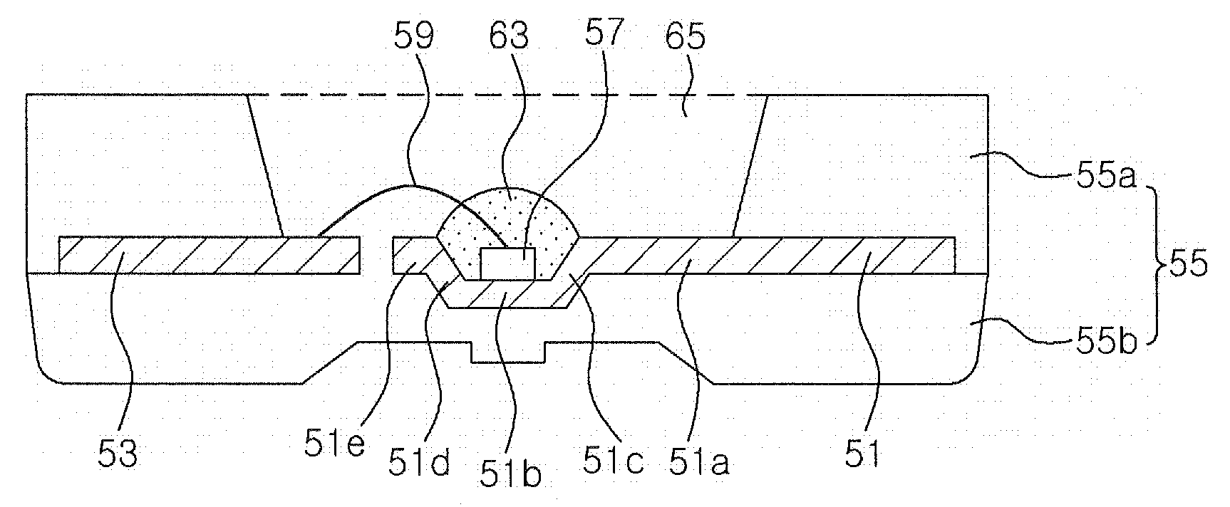
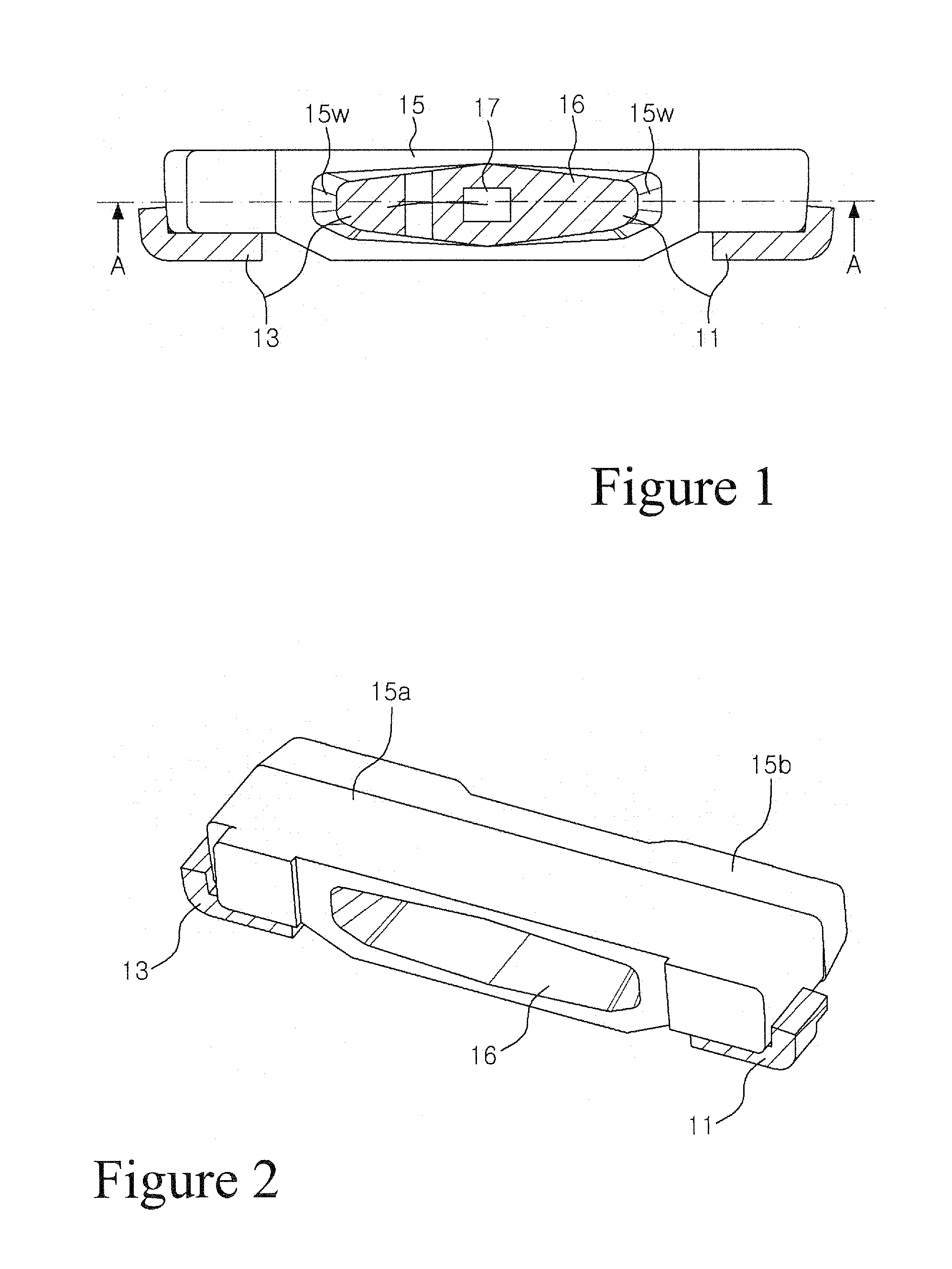
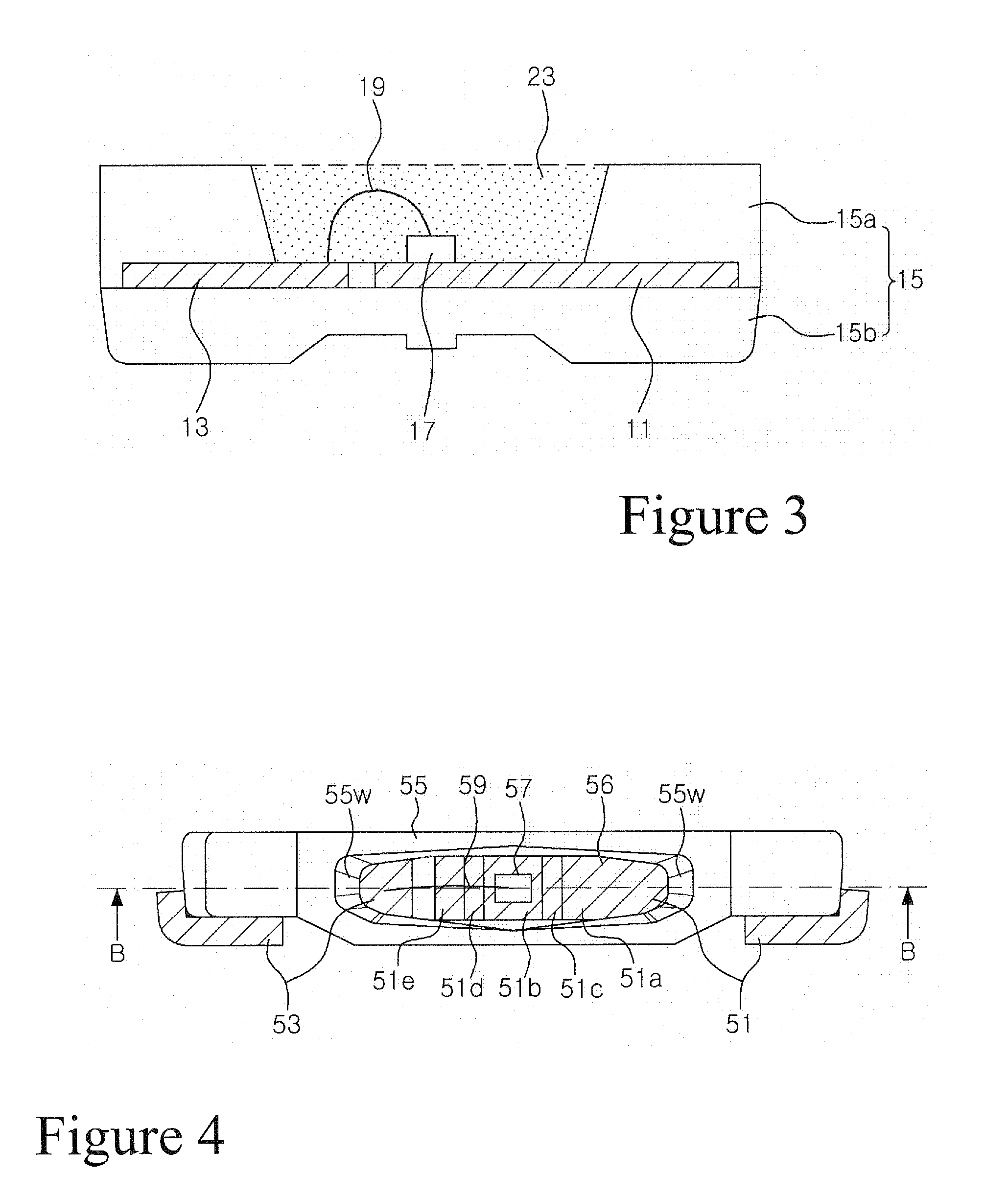
[0046]FIG. 4 is a plan view illustrating a side-view LED package according to an embodiment of the present invention, FIG. 5 is a sectional view taken along line B-B in FIG. 4, FIG. 6 illustrates a variety of first lead terminals applicable to a side-view LED package according to embodiments of the present invention, and FIG. 7 illustrates a first lead terminal applicable t...


PUM


Abstract

Disclosed is a light emitting diode (LED) package employing a lead terminal with a reflecting surface. The package includes first and second lead terminals that are spaced apart from each other. The first lead terminal has a lower portion with an LED chip mounting area, and at least one reflecting surface formed by being bent from the lower portion. Meanwhile, a package body supports the first and second lead terminals and forms a cavity through which the LED chip mounting area and the reflecting surface of the first lead terminal and a part of the second lead terminal are exposed. The first and second lead terminals extend outside of the package body. Accordingly, light emitted from an LED chip can be reflected on the reflecting surface with high reflectivity, so that the optical efficiency of the package can be improved.

Description

CROSS-REFERENCE TO RELATED PATENT APPLICATION[0001]This application claims the benefit of Korean Patent Application No. 10-2006-0079792, filed on Aug. 23, 2006, and Korean Patent Application No. 10-2007-0036516, filed on Apr. 13, 2007, in the Korean Intellectual Property Office, the disclosures of which are incorporated herein in their entirety by reference.TECHNICAL FIELD[0002]The present invention relates to a light emitting diode package, and more particularly, to a light emitting diode package employing a lead terminal with a reflecting surface.BACKGROUND ART[0003]Generally, light source systems using light emitting diode (LED) chips are constructed by mounting LED chips in various kinds of packages according to desired uses of the systems. A side-view LED package is disposed at a lateral side of a light guiding plate to provide light in parallel to the light guiding plate. Thus, the side-view LED package is mainly used for backlight illumination for a variety of displays.[0004]...

Claims


Application Information

Patent Timeline
Patent Type & Authority Applications(United States)
IPC IPC(8): H01L33/00H01L33/56H01L33/50H01L33/60H01L33/62H01L33/64
CPCH01L33/483H01L33/60H01L33/62H01L2224/48091H01L2224/48247H01L2924/01079H01L2924/01012H01L2924/00014
Inventor KIM, HWA JAKIM, NAM YOUNGLEE, MYUNG HEEHAN, KYOUNG BOKIM, TAE KWANGSO, JI SEOP
Owner SEOUL SEMICONDUCTOR
Why Eureka
Try Eureka