

Liquid crystal display device having delay compensation
a delay compensation and display device technology, applied in static indicating devices, instruments, non-linear optics, etc., can solve problems such as undesirable degradation of image quality
- Summary
- Abstract
- Description
- Claims
- Application Information
AI Technical Summary
Benefits of technology
Problems solved by technology
Method used
Image

Examples
first embodiment
[0059]Hereinafter, the first substrate 100 will be described.
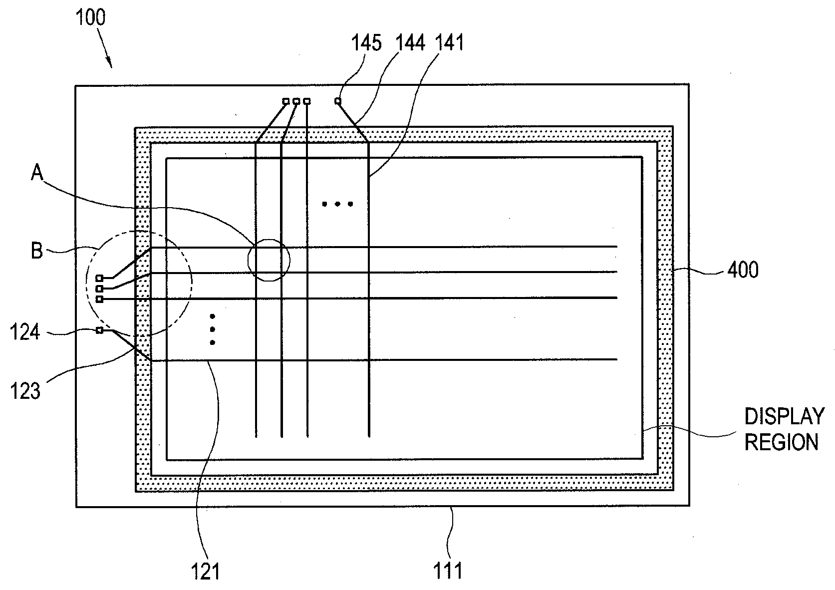
[0060]A gate signal is transmitted from a signal origination pad (e.g., IC connection pad, see 124 of FIG. 7) to gate electrode over a gate wire where the latter wire is formed on a first insulating substrate 111. The gate wire may include a single or plural metal layers. The gate wire generally includes the gate main line 121 which is disposed in the display region and extends transversely, the gate electrode 122 which is connected with the gate main line 121, the fan-out part 123 which extends from the gate main line 121 to the non-display region, and the gate pad 124 which is connected with an end part of the fan-out part 123. A storage electrode line 125 often extends in parallel with the gate main line 121 as seen for example in FIG. 2.
[0061]The gate signal origination pad 124 is often connected with a packaging terminal or IC pin of a gate driver circuit (not shown) that outputs the gate signal to the pad end of the...
third embodiment
[0120]Hereinafter, a liquid crystal display device according to the present disclosure will be described with reference to FIGS. 16 and 17.
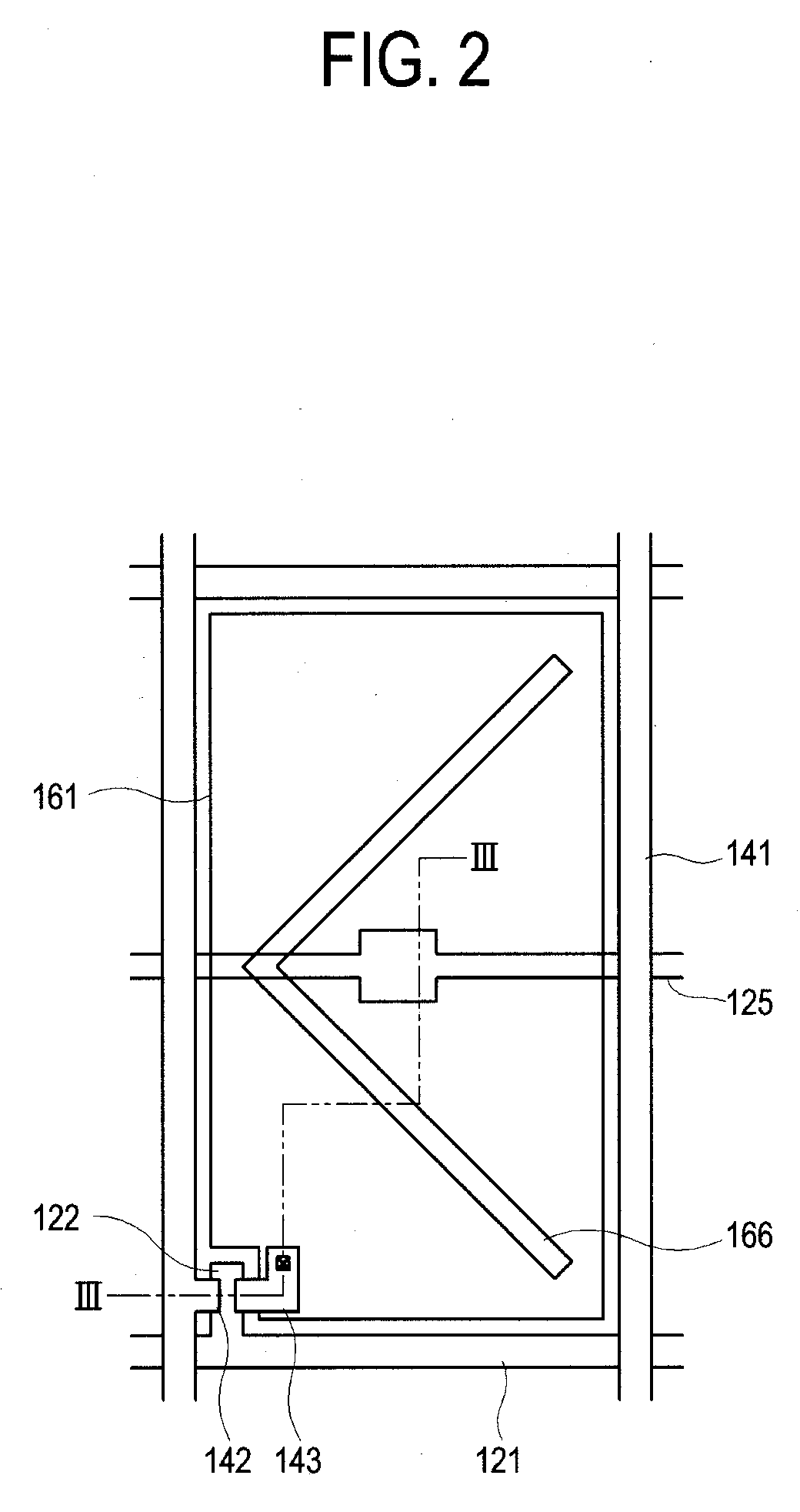
[0121]A gate pad 164 and a fan-out part 165 according to the third embodiment are integrally formed in a same layer with the ballasting resistor 163. The gate pad 164 and the fan-out part 165 may include indium tin oxide (ITO) or indium zinc oxide (IZO). The resistor 163 is connected with a gate main line 121 through a contact hole 156. The gate pad 164 and the fan-out part 165 perform the same operation as the resistor 163 according to the first embodiment.
[0122]In one embodiment, the resistance of the ballasting resistor 163 is in inverse proportion to a distance between the corresponding gate main line 121 and the gate pad 164 as was the case for one version of the first embodiment. Thus, brightness irregularity due to a distance difference between the gate main line 121 and the gate pad 164 decreases.
[0123]In another embodiment of the present...
fourth embodiment
[0124]A liquid crystal display device will be described with reference to FIGS. 18 to 20.
[0125]As shown in FIG. 18, a thin film transistor T is connected with two liquid crystal capacitances CLC1 and CLC2. The first liquid crystal capacitance CLC1 is formed between a first pixel electrode PE1 and a common electrode CE. The first pixel electrode PE1 is directly connected with the thin film transistor T. The second liquid crystal capacitance CLC2 is formed between the second pixel electrode PE2 and the common electrode CE. The second pixel electrode PE2 is indirectly connected with the thin film transistor T through a coupling capacitance CCP.
[0126]Here, the first pixel electrode PE1 and the second pixel electrode PE2 are electrically separated from each other due to the presence of coupling capacitance CCP and the second liquid crystal capacitance CLC2.
[0127]The liquid crystal display device according to the fourth embodiment can improve visibility per a mechanism which will be desc...
PUM
| Property | Measurement | Unit |
|---|---|---|
| kick back voltage | aaaaa | aaaaa |
| kick back voltage | aaaaa | aaaaa |
| kick back voltage | aaaaa | aaaaa |
Abstract
Description
Claims
Application Information