Liquid crystal display device and video display device

a display device and liquid crystal technology, applied in static indicating devices, instruments, non-linear optics, etc., can solve the problems of increasing the number of manufacturing processes, difficult to control the state of the film, and low feasibility, so as to prevent display defects, suppress the effect of ionic impurity, and improve image quality

Active Publication Date: 2008-03-06
SONY CORP
View PDF6 Cites 54 Cited by
  • Summary
  • Abstract
  • Description
  • Claims
  • Application Information

AI Technical Summary

Benefits of technology

[0017]The proposition to use a special material increases the number of manufacturing processes and is thus low in feasibility.
[0021]It is desirable to provide a liquid crystal display device and a video display device that can suppress the effect of an ionic impurity within a liquid crystal cell, prevent display defects such as burn-in and the like, and in turn obtain higher image quality.
[0026]According to an embodiment of the present invention, it is possible to suppress the effect of an ionic impurity within a liquid crystal cell, prevent display defects such as burn-in and the like, and in turn obtain higher image quality.

Problems solved by technology

However, with a technique for changing the state of the alignment film in the peripheral area, it is very difficult to control the state of the film.
The proposition to use a special material increases the number of manufacturing processes and is thus low in feasibility.
The proposition to provide a projection provides insufficient effect because it is difficult to completely keep away the impurity eluted in a liquid crystal.

Method used


Image

  • Liquid crystal display device and video display device
  • Liquid crystal display device and video display device
  • Liquid crystal display device and video display device

Examples


examples of modification

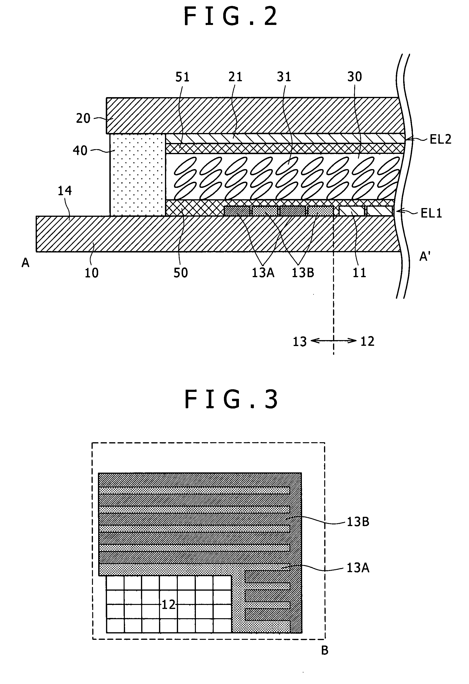
[0106]In the present embodiment, the TFT substrate 10 is a transparent substrate. However, the TFT substrate 10 may be formed as a reflection substrate on which reflection type pixel electrodes are arranged, using a silicon (Si) substrate.

[0107]In addition, in the constitution of FIG. 2, an example is shown in which a plurality of peripheral electrodes 13A and 13B adjacent to each other are provided in the peripheral area 13 of the TFT substrate 10 as a first substrate. However, as shown in FIG. 10, for example, a second electrode part EL2A can be formed on the side of the counter substrate 20 as a second substrate by providing a common electrode (pixel electrode part) 21A in the pixel area 12 and a plurality of peripheral electrodes 21B and 21C adjacent to each other in the peripheral area 13 as in the case of the TFT substrate 10 in place of the common electrode.

[0108]In this case, driving voltage is applied to the peripheral electrodes 21B and 21C in the same manner as the drivin...


PUM

PropertyMeasurementUnit
Frequencyaaaaaaaaaa
Voltageaaaaaaaaaa
Voltageaaaaaaaaaa

Abstract

Disclosed herein is a liquid crystal display device. The liquid crystal display device includes: a first substrate; a second substrate; a liquid crystal layer; a first electrode part; and a second electrode part. The first electrode part includes a pixel electrode formed in the pixel area and a peripheral electrode formed in the peripheral area. The second electrode part includes a pixel electrode part formed in the pixel area and a peripheral electrode formed in the peripheral area. The peripheral electrode of at least one of the first electrode part and the second electrode part is formed by a plurality of electrodes adjacent to each other. Voltage values of driving voltages applied to the respective electrodes adjacent to each other of the peripheral electrode are different from each other.

Description

CROSS REFERENCES TO RELATED APPLICATIONS[0001]The present invention contains subject matter related to Japanese Patent Application JP 2006-233909 filed with the Japan Patent Office on Aug. 30, 2006, the entire contents of which being incorporated herein by reference.BACKGROUND OF THE INVENTION[0002]1. Field of the Invention[0003]The present invention relates to a liquid crystal display device and a video display device, and particularly to a liquid crystal display device and a video display device having a liquid crystal panel that can suppress degradation in display characteristics in the liquid crystal panel.[0004]2. Description of the Related Art[0005]A projection type video display device such as a liquid crystal projector or the like separates light emitted from a light source into red, green, and blue, modulates the pieces of color light by three light valves formed by a liquid crystal display element, synthesizes color luminous fluxes after the modulation, and then enlarges a...

Claims


Application Information

Patent Timeline
Patent Type & Authority Applications(United States)
IPC IPC(8): G02F1/1343G02F1/1335
CPCG02F1/134309G02F2001/133388G09G2320/043G09G2300/0426G09G2320/0257G09G3/3655G02F1/133388G02F1/133
Inventor SHIRASAKA, YASUHIROUEDA, KAZUYAFUKUMOTO, HIROHIDEKADOTA, HISASHI
Owner SONY CORP
Why Eureka
Try Eureka