Application processor circuit incorporating both sd host and slave functions and electronic device including same

a technology of application processor and slave function, which is applied in the direction of instruments, coding, code conversion, etc., can solve the problems of inability to enable data exchange between two pda devices and inability to achieve interconnection therebetween via such interfaces

Inactive Publication Date: 2008-03-06
NORTH STAR INNOVATIONS
View PDF15 Cites 25 Cited by
  • Summary
  • Abstract
  • Description
  • Claims
  • Application Information

AI Technical Summary

Problems solved by technology

Existing application processor chips supporting the SD interface only include SD host logic to support SD slave device, but cannot achieve interconnection therebetween via such interfaces...

Method used


Image

  • Application processor circuit incorporating both sd host and slave functions and electronic device including same
  • Application processor circuit incorporating both sd host and slave functions and electronic device including same
  • Application processor circuit incorporating both sd host and slave functions and electronic device including same

Examples


Embodiment Construction

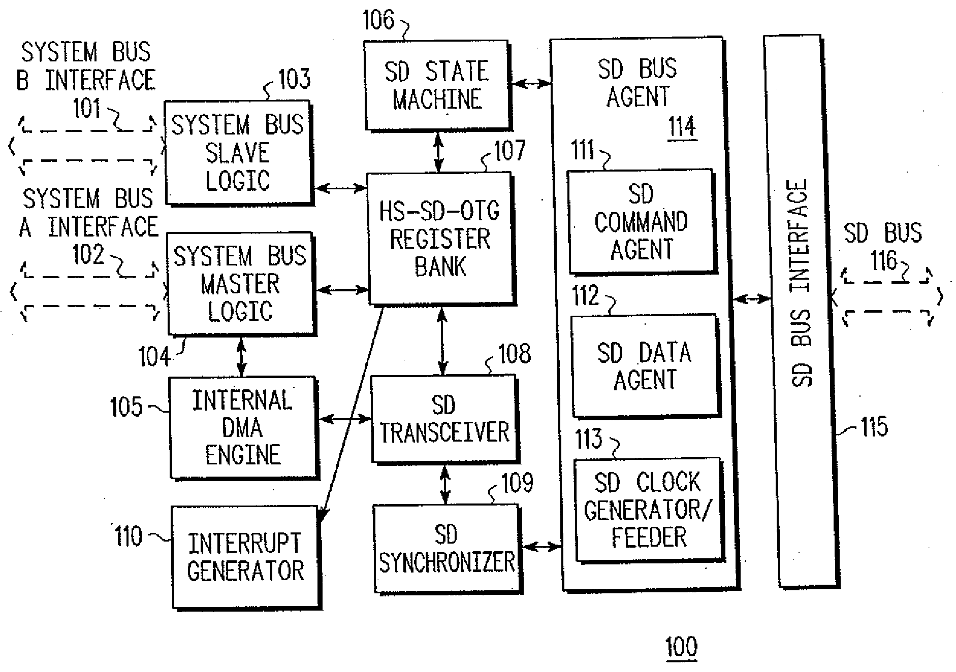
[0024]FIG. 1 illustrates generally the architecture of an application processor circuit 100 according to one embodiment of the present invention. The circuit 100 works in two bus domains, i.e., the system bus domain shown on the left side, and the SD bus domain shown on the right side of FIG. 1. In FIG. 1, system bus A interface 102 is used for data transfer. System bus A interface 102 is connected to system bus master logic 104. In FIG. 1, system bus B interface 101 is used for the configuration of a register bank (the configuration of the register bank is explained below). The system bus B interface 101 is connected to system bus slave logic 103. During data transfer by means of system bus A, system bus master logic 104 is used to select the devices on system bus A with which it conducts data transfer and is used to start data transfer. In one embodiment, separate system buses A and B are used respectively for configuration of functional modules and data transfer, to improve perfo...


PUM


Abstract

An application processor circuit has SD-compatible interface protocols and can perform both host and slave functions. The circuit includes SD bus interface logic for realizing SD interface signals defined in SD-compatible interface protocols; system bus interface logic for performing the interface function on the system bus side; a data buffer for adjusting the data transfer rate difference between the SD bus interface and the system bus interface; a data buffer controller for controlling access to the data buffer; and a configuration unit for configuring the circuit to work in the host mode or slave mode. The SD-compatible interface protocols include MMC/SD/SDIO protocol, high speed MMC/SD/SDIO protocol, and CE-ATA interface protocol. The SD host logic and slave logic are incorporated in a single module to support both the SD host and slave functions, so as to achieve more convenient data transfer between electronic devices.

Description

BACKGROUND OF THE INVENTION[0001]The present invention relates to high speed data transfer between electronic devices. More specifically, the present invention relates to an application processor circuit compliant with MMC / SD / SDIO protocol, and to a portable electronic device including the application processor circuit.[0002]The application processors in more and more portable electronic devices, e.g., personal digital assistance (PDA), portable music player and notebook computer, support interfaces compliant with MMC / SD / SDIO protocol, since these interfaces can achieve high efficiency in data transfer and are easy to use. The PDA devices, for example, implement some functions by means of external cards connected via an SD card slot to provide a variety of choices to the user and enable the user to configure the PDA device. These functions not only include expansion of the memory capacity of the PDA device, but also include other PDA functions that support connections with various o...

Claims


Application Information

Patent Timeline
IPC IPC(8): G06F13/14H03M13/09
CPCG06F13/4059
Inventor ZHANG, LIWEI, SU-FENXIAO, YAN
Owner NORTH STAR INNOVATIONS
Why Eureka
Try Eureka