Schema-based portal architecture for assessment and integration of silicon IPs

a portal architecture and silicon ips technology, applied in the field of silicon intellectual property (ip) based integrated circuit (ic) design, can solve the problems of increasing labor and time consumption of integrating complex silicon ip blocks into a system, complex design of integrated circuit (ic) chips such as application-specific ics (asics) and system-on-chips, and increasing the difficulty of managing a large number of ip blocks from multiple ip vendors in various design languages and data

Inactive Publication Date: 2007-08-30
IBM CORP
View PDF29 Cites 53 Cited by
  • Summary
  • Abstract
  • Description
  • Claims
  • Application Information

AI Technical Summary

Benefits of technology

[0021]FIG. 9B depicts a mode of operation for internal or external users to utilize functions of an IP portal with access to one or more third party portals and repositories according to some embodiments; and

Problems solved by technology

Design of an Integrated Circuit (IC) chip such as Application-Specific ICs (ASICs) and system-on-chips (SoC's) is a very complex, expensive, and time-consuming task.
While using IP blocks in a design can provide significant efficiencies when compared with designing a chip at the transistor level or gate level, management of a large number of IP blocks from multiple IP vendors in various design languages and databook format and configurations has its own complexities.
As ASICs, SoCs and other designs grow larger and more sophisticated, the task of integrating complex silicon IP blocks into a system becomes increasingly labor intensive and time consuming.
Additionally, the number and complexity of IPs used in SoCs and ASICs is also increasing as designers are more and more frequently taking advantage of IPs for SoC or ASIC designs.
The percentage of total IC area taken by IP designs is also increasing due to the increasing complexity of IP designs.
The difficulty in integrating IPs is exacerbated by the fact that for most designs the majority of the IPs are developed by third party IP developers.
The use of third party IPs complicates the task of integration of these IPs into the design because of concern about maintaining confidentiality of information and protecting intellectual property rights and because of different design styles and ad hoc verification of non-standard databooks and delivery packages, often resulting in a failure of third party IPs to meet internal requirements.
This often results in additional resources being required to evaluate and validate third party IPs and, in many cases, in-house designers must spend more time verifying an IP than it took to develop in the first place.
This process, however, is currently error-prone and ad hoc as SoC and ASIC designers must manually evaluate each IP for compliance with rules, tools, or other organizational requirements, a time-consuming and expensive process.
Many of the organization's own standards, however, must be kept confidential and proprietary, making it difficult for third party IP developers to ensure that their IPs conform to the organization's requirements.

Method used


Image

  • Schema-based portal architecture for assessment and integration of silicon IPs
  • Schema-based portal architecture for assessment and integration of silicon IPs
  • Schema-based portal architecture for assessment and integration of silicon IPs

Examples


Embodiment Construction

[0023] The following is a detailed description of example embodiments of the invention depicted in the accompanying drawings. The example embodiments are in such detail as to clearly communicate the invention. However, the amount of detail offered is not intended to limit the anticipated variations of embodiments; but, on the contrary, the intention is to cover all modifications, equivalents, and alternatives falling within the spirit and scope of the present invention as defined by the appended claims. The detailed descriptions below are designed to make such embodiments obvious to a person of ordinary skill in the art.

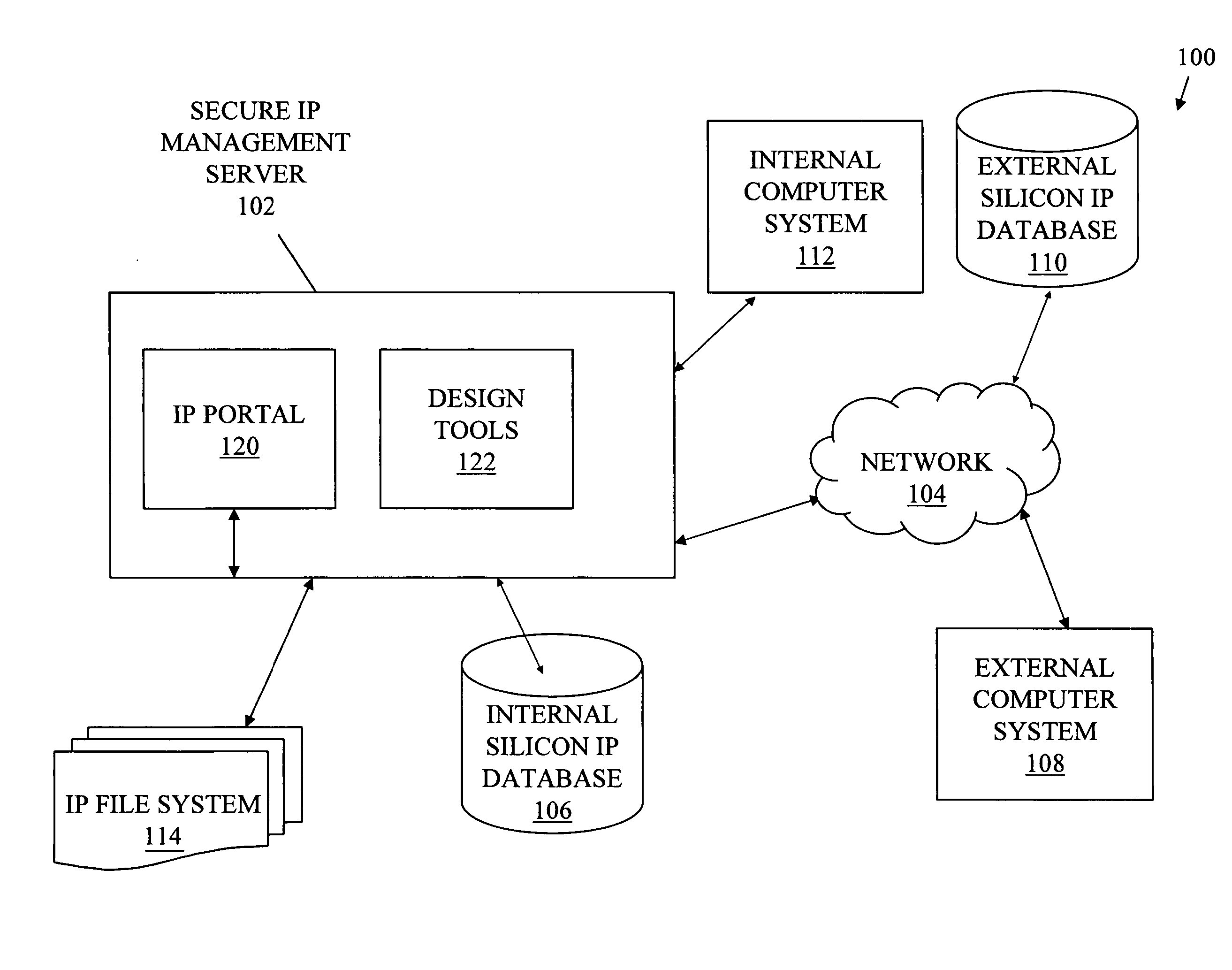
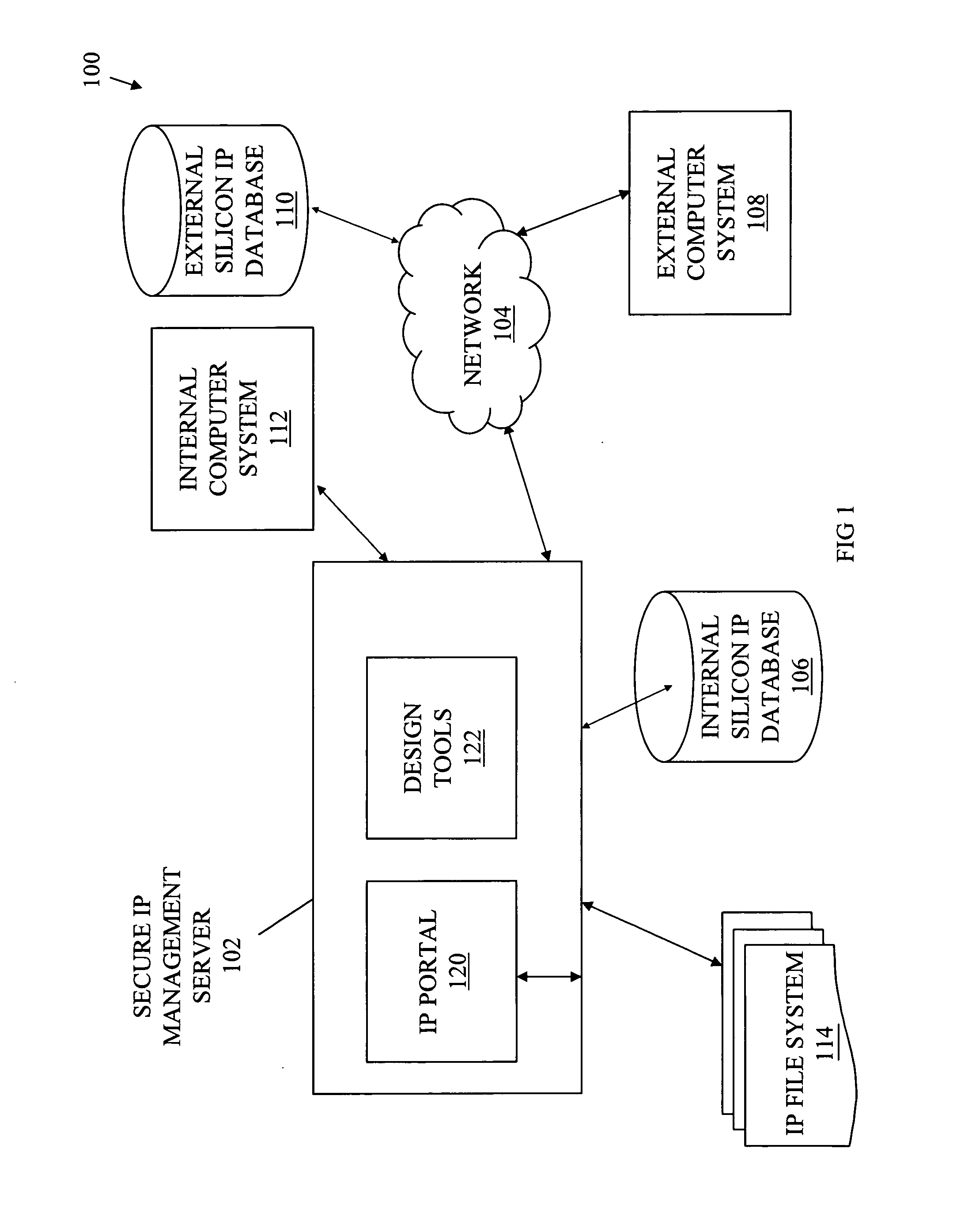
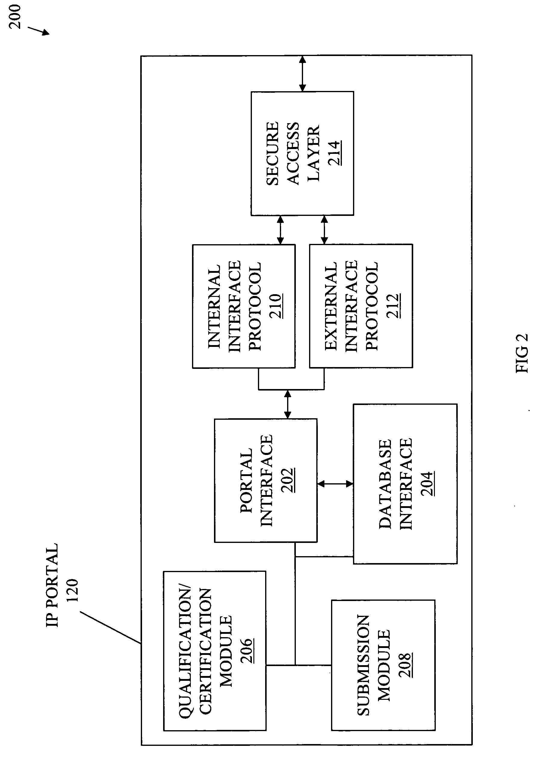
[0024] Generally speaking, systems, methods, and media for a schema-based portal architecture for assessment and integration of silicon IPs are disclosed. Embodiments may generally include an IP portal system having a portal interface to receive inputs from one or more users, design platforms, or IP portals and to provide output to one or more users, design platform...


PUM


Abstract

Systems, methods, and media for a schema-based portal for assessment and integration of silicon IPs are disclosed. Embodiments may generally include an IP portal system having a portal interface to receive inputs from users and to provide output to users and a database interface to transmit and receive information to and from a silicon IP database and an IP file system. Embodiments of the system may also include a secure access layer (HTTP tunnel, firewall, or proprietary secure access protocol) to securely communicate information and an internal interface protocol and an external interface protocol and the secure access layer. The internal interface protocol may authorize and encrypt communications to an internal user or design system and the external interface protocol may authorize and encrypt communications to an external user or design system. The portal interface may be a Web-based interface and schema-based in some embodiments.

Description

FIELD OF INVENTION [0001] The present invention generally relates to the field of silicon intellectual property-(IP-) based integrated circuit (IC) design. More particularly, the present invention relates to systems, methods, and media for schema-based portal architecture for assessment of silicon IPs for integration with an organization's proprietary in-house design flow for IC chip or other silicon designs. BACKGROUND [0002] Design of an Integrated Circuit (IC) chip such as Application-Specific ICs (ASICs) and system-on-chips (SoC's) is a very complex, expensive, and time-consuming task. To help streamline this task, designers often utilize silicon IPs (also known as intellectual property blocks, IP cores, or integrated circuit macros) to facilitate the design task. IPs are units of reusable design whose use may have been licensed from a third party IP vendor. IPs may represent design components such as processor units, interface protocols, data storage elements, functions, etc. t...

Claims


Application Information

Patent Timeline
Patent Type & Authority Applications(United States)
IPC IPC(8): H04L12/66
CPCH04L12/4633
Inventor HEKMATPOUR, AMIRSALEHI, AZADEH
Owner IBM CORP
Why Eureka
Try Eureka