

Ion beam monitoring in an ion implanter using an imaging device
- Summary
- Abstract
- Description
- Claims
- Application Information
AI Technical Summary
Benefits of technology
Problems solved by technology
Method used
Image

Examples
Embodiment Construction
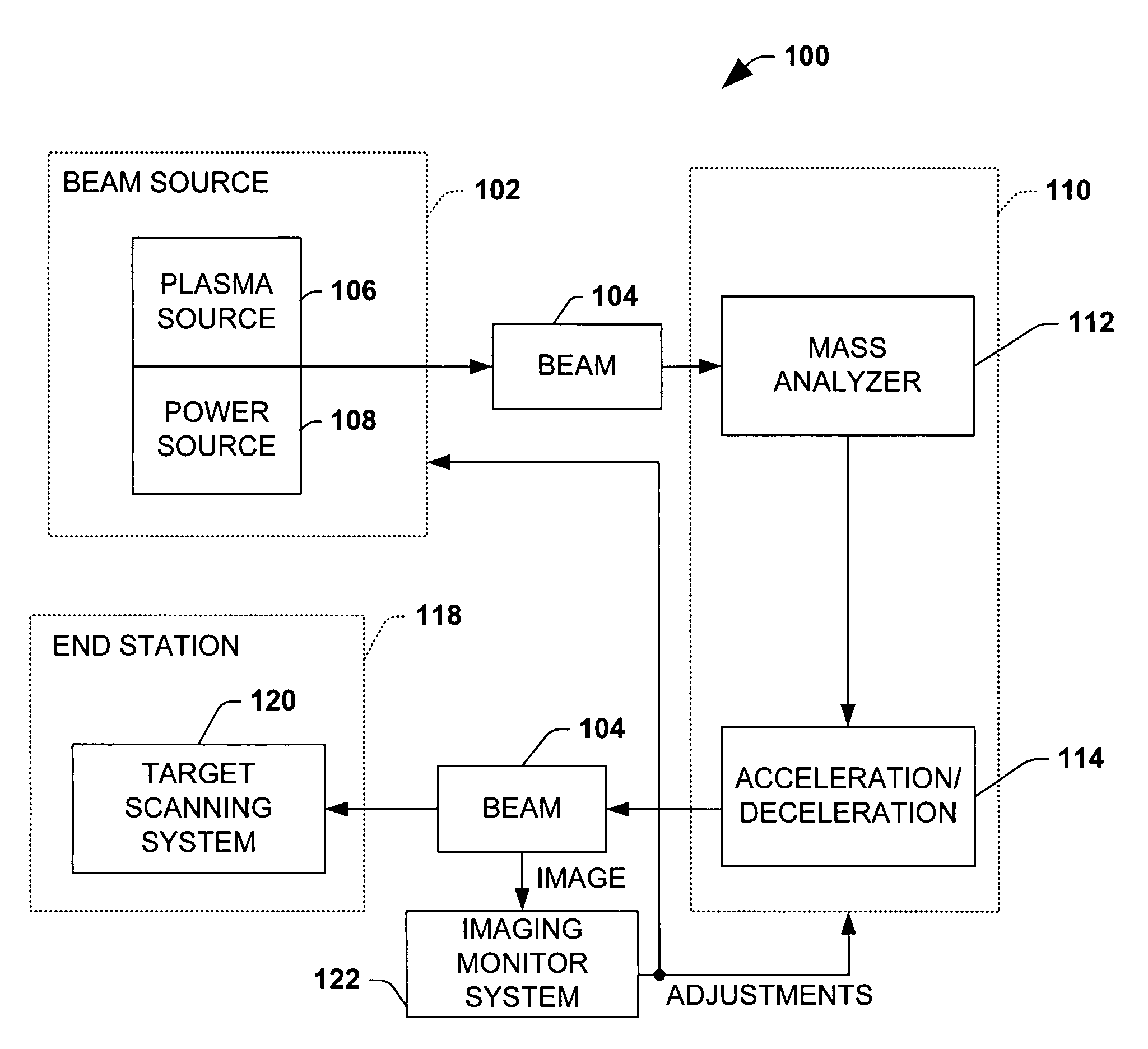
[0020]The present invention will now be described with reference to the attached drawings, wherein like reference numerals are used to refer to like elements throughout. It will be appreciated by those skilled in the art that the invention is not limited to the exemplary implementations and aspects illustrated and described hereinafter.
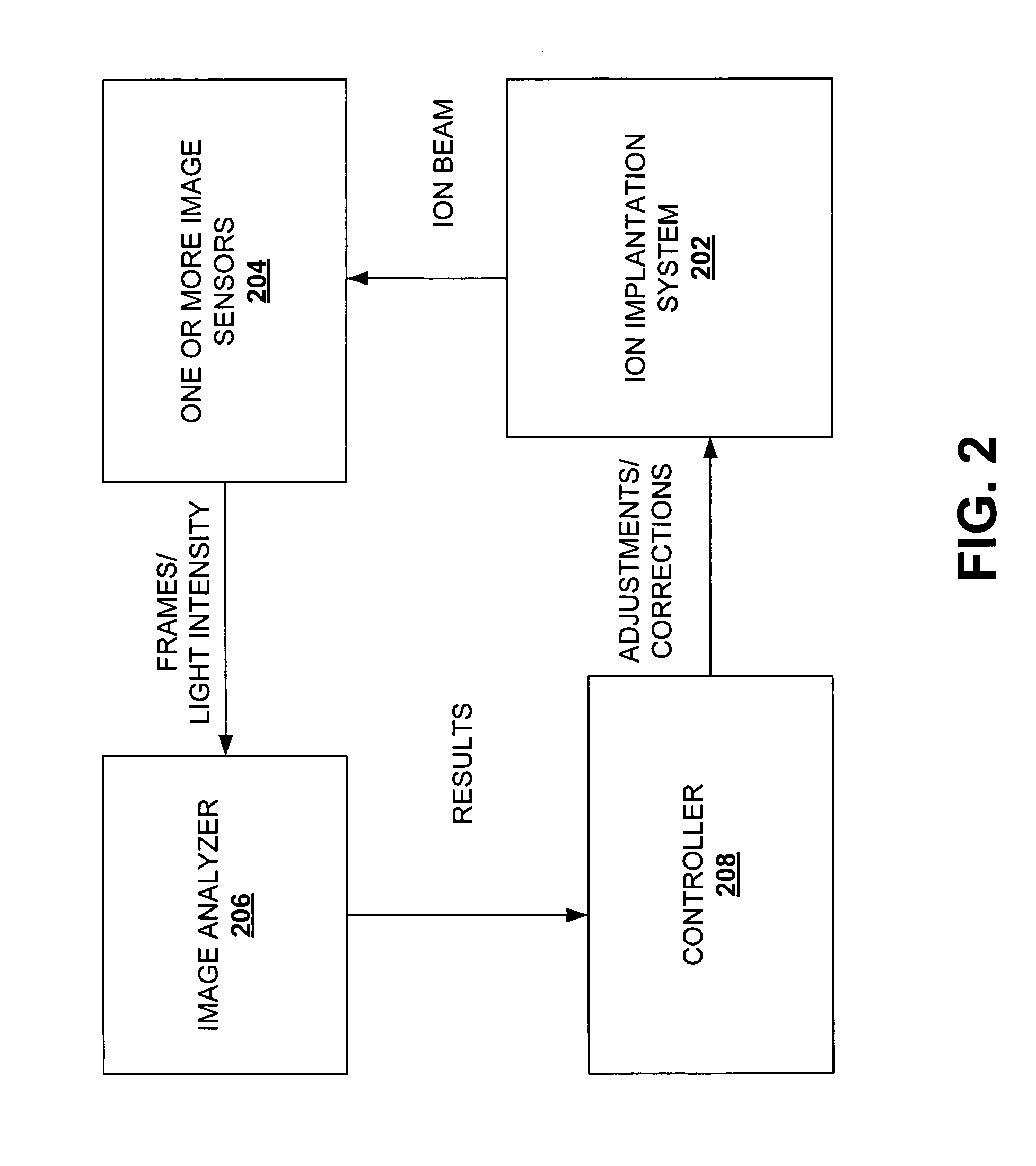
[0021]Aspects of the present invention facilitate ion implantation processes and systems by monitoring ion beam characteristics during ion implantation and permitting correction adjustment to the ion beam generation and formation in real time. Orthogonal or cross sectional images of the ion beam are obtained at various times and subsequently analyzed to identify beam characteristics. These identified characteristics can then be compared with desired or expected characteristics. Deviations there from can result in corrective adjustments to move future measured characteristics to be toward the desired or expected characteristics.
[0022]Referring initiall...
PUM
 Abstract
Description
Claims
Application Information