Method for connecting a contactless integrated circuit to a NFC component

a contactless integrated circuit and component technology, applied in the field of nfc technology, can solve the problems of slow and low adaptability to high-rate data received by the component nfcm, high electrical consumption, and low efficiency of the integrated circuit, so as to rationalize the production of integrated circuits

Inactive Publication Date: 2008-03-13
INSIDE CONTACTLESS SA
View PDF0 Cites 43 Cited by
  • Summary
  • Abstract
  • Description
  • Claims
  • Application Information

AI Technical Summary

Benefits of technology

[0020]More particularly, embodiments of the present invention are directed to a device for exchanging data with a contactless integrated circuit, minimizing the modifications to be made to the integrated circuit, in order to rationalize the production of integrated circuits.

Problems solved by technology

Determining a “universal” communication protocol between the component NFCM and the integrated circuit IC does not seem possible in practice as it faces a problem of rationalization of the industrial production of integrated circuits.
The ISO 7816 bus however has the drawback of being slow and little adapted to high rate transfers of the data received by the component NFCM by means of its contactless communication interface.
In addition, the interface S2C components, on either side of the bus S2C, switch at high rate and have a high electrical consumption.
Eventually, the bus S2C does not enable energy to be transferred.

Method used


Image

  • Method for connecting a contactless integrated circuit to a NFC component
  • Method for connecting a contactless integrated circuit to a NFC component
  • Method for connecting a contactless integrated circuit to a NFC component

Examples


embodiment 1

, FIG. 13

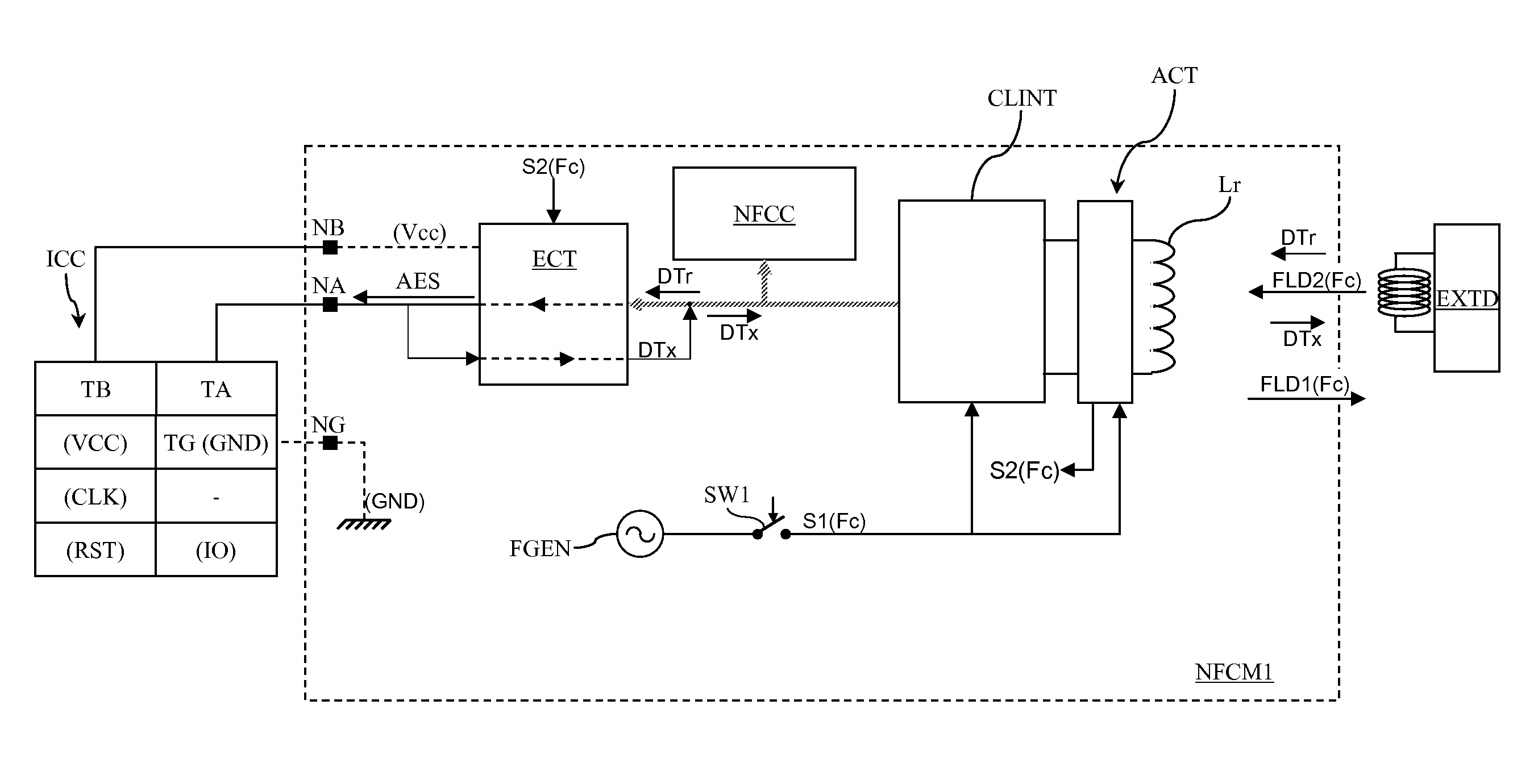
[0156]In FIG. 13, the NFC component, designated “NFCM2”, is provided to receive another host processor HP2. It allows a communication to be established between, on the one hand the external device EXTD and on the other hand, the host integrated circuit ICC or the host processor HP2.

[0157]Performing the application concerned, for example an application of AP2 type, can for example be entrusted to the integrated circuit ICC if it is secure and if the application is not free or requires access conditions to secure (subscription for example). Performing the application can also be entrusted to the processor HP2 if it is not secure and if the application is free and without secure access condition. The processor HP2 can also be used to manage applications of AP1 or AP3 type (FIG. 2).

[0158]To that end, the outgoing data DTx carrier signal SDTx as applied to the circuit RFMOD can be supplied by the processor HP2, for example via the controller NFCC, or by the integrated circuit IC...

embodiment 2

, FIG. 14

[0160]In FIG. 14 the NFC component, designated “NFCM3”, differs from the component NFCM1 in that the NFC controller is interposed in the incoming and outgoing data flow. The incoming data carrier signal supplied by the demodulation circuit RFDEM to the controller NFCC is designated SDTr1 whereas the incoming data carrier signal supplied by the controller NFCC to the interface circuit ECT is designated SDTr2. Likewise, the outgoing data carrier signal supplied by the interface circuit ECT to the controller NFCC is designated SDTx1 and the outgoing data carrier signal supplied by the controller NFCC to the modulation circuit RFMOD is designated SDTx2.

[0161]The signal SDTr1 can be processed or not by the controller NFCC. If the controller NFCC sends the signal SDTr1 back to the interface circuit ECT as it is (SDTr2=SDTr1), the operating mode obtained is therefore identical to that of FIG. 7 (component NFCM3 transparent to the host integrated circuit). The controller NFCC can a...

embodiment 3

, FIGS. 15 and 16

[0164]The embodiment shown in FIG. 15 of the NFC component according to the invention, designated “NFCM4”, forms an entity of computational type in which data circulate on a data bus DTB associated to an address bus ADB, the data and address buses being controlled by the controller NFCC. In this embodiment, the interface circuit ECT according to the invention is a peripheral element of the controller NFCC.

[0165]The Component NFCM4 More Particularly Comprises:

[0166]the controller NFCC and the interface circuit CLINT already described;

[0167]a memory array comprising for example a program memory MEM1 (ROM memory), a volatile data memory MEM2 (RAM) and an electrically erasable and programmable data memory MEM3 (EEPROM);

[0168]a communication port INT1 of UART type, to which a host processor HP3 can be connected;

[0169]a communication port INT2 of ISO 7816 type to which a host processor HP2 can be connected (for example a SIM card);

[0170]a connection port INT3 / ECT accordin...


PUM


Abstract

A method for exchanging data with an integrated circuit includes antenna connection terminals. The method includes not connecting the antenna connection terminals of the integrated circuit to an antenna, applying an alternating emulation signal at least to a first antenna connection terminal of the integrated circuit, by way of a wire link, in order to emulate the presence of an antenna signal on the first antenna connection terminal, sending data to the integrated circuit by injecting them in the emulation signal, and receiving data sent by the integrated circuit by taking them from the emulation signal.

Description

BACKGROUND OF THE INVENTION[0001]Embodiments of the present invention are related to the development and improving of the NFC technology (Near Field Communication).[0002]The NFC technology is currently developed by an industry consortium under the name of NFC Forum (http: / / www.nfc-forum.org). The NFC technology derives from Radio Frequency Identification technology (RFID) and uses NFC components having a contactless communication interface (contactless data sending / receiving) and several operating modes, i.e., a “reader” mode, a “card emulation” mode, and a “device” mode (or “device-to-device”). In the reader mode, the NFC component operates as a conventional RFID reader to read or write access to a RFID chip (chip card or contactless tag in particular). It emits a magnetic field, sends data by modulating the amplitude of the magnetic field and receives data sent by retromodulation (charge modulation). In the emulation mode, described by European Patent No. EP 1 327 222 in the name ...

Claims


Application Information

Patent Timeline
Patent Type & Authority Applications(United States)
IPC IPC(8): H03D7/16
CPCG06K7/0008G06K7/10237G06K19/0723G06K19/0722G06K19/06206
Inventor CHARRAT, BRUNO
Owner INSIDE CONTACTLESS SA
Why Eureka
Try Eureka