Sample and method for evaluating resolution of scanning electron microscope, and electron scanning microscope

a scanning electron microscope and resolution technology, applied in the field of electron scanning microscopes, can solve the problems of inability to prepare such samples, difficulty in directly measuring the size of electron beams, etc., and achieve the effects of improving the resolution of scanning electron microscopes, reducing the difficulty of direct measurement of electron beams, and improving the degree of accuracy

Inactive Publication Date: 2008-03-20
HITACHI HIGH-TECH CORP
View PDF4 Cites 4 Cited by
  • Summary
  • Abstract
  • Description
  • Claims
  • Application Information

AI Technical Summary

Benefits of technology

[0023]According to the present invention, the scanning electron microscope with the use of a sample for evaluating a resolution can measure a resolution with a higher degree of accuracy, and as a result, a variation in resolution of a scanning electron microscope and differences in resolution among scanning electron microscopes can be managed with a high degree of accuracy. Thus, it is possible to measures dimensions with a higher degree of reliability and a high degree of accuracy during, for example, a process of manufacturing a semiconductor pattern, resulting in an improvement in performance of a product and in an improvement in the yield thereof.

Problems solved by technology

However, it is difficult to directly measure a size of an electron beam.
However, it is impossible to prepare such a sample, and the following problem will be caused.
In view of the above-mentioned matters regarding the resolution monitor, a resolution problem inevitably has such a task that the preparation of a sample and the utilization of a measurement algorithm, which are capable of reducing the pattern dependency of an index value of resolution to be measured are required for precisely measuring a variation in size of an electron beam.

Method used


Image

  • Sample and method for evaluating resolution of scanning electron microscope, and electron scanning microscope
  • Sample and method for evaluating resolution of scanning electron microscope, and electron scanning microscope
  • Sample and method for evaluating resolution of scanning electron microscope, and electron scanning microscope

Examples


Embodiment Construction

[0044]Explanation will be hereinbelow made of an embodiment of the present invention with reference to the accompanying drawings.

[0045]In this embodiment, an image of a sample for evaluating a resolution, which has been obtained by a scanning electron microscope, is evaluated in order to evaluate and manage a resolution of the above microscope.

[0046](0) Sequence

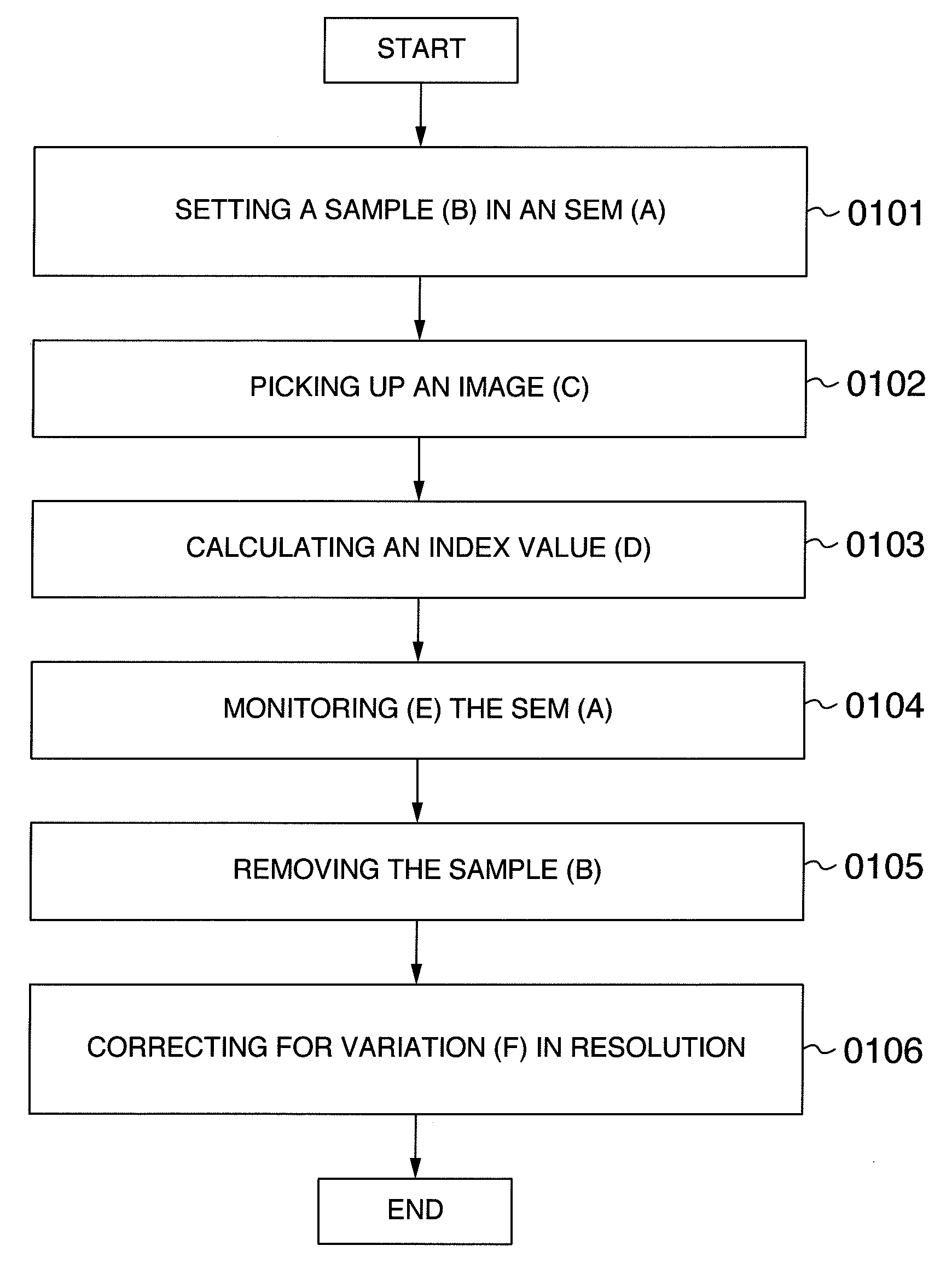
[0047]Referring to FIG. 1 which shows a sequence for evaluating a resolution, according to the present invention, the sequence comprises, at first, a step 0101 of setting a sample (B) for evaluating a resolution, onto a scanning electron microscope (A) whose resolution is to be evaluated, a step 0102 of picking up an image (C) of the sample (B) for evaluating a resolution, a step 0103 of calculating an index value (D) of resolution of the microscope from the picked-up image (C), a step 0104 of then storing the thus calculated index value (D) of resolution for each microscope and for each time series in order to monitor a cond...


PUM

PropertyMeasurementUnit
sizeaaaaaaaaaa
diverging angleaaaaaaaaaa
relative angleaaaaaaaaaa

Abstract

In the case of monitoring a resolution of a scanning electron microscope, it is required to prepare a sample and to use a measuring algorithm so as to reduce the pattern dependency of an index value of resolution to be measured in order to measure a variation in the size of an electron beam with a high degree of accuracy. According to the present invention, there is used a sample having a sectional shape which is appropriate for monitoring the resolution, that is, the sample has a pattern with such a sectional shape that a side wall of the pattern is inclined so as to prevent an electron beam irradiated on the sample from impinging upon the side wall of the pattern. With this configuration, it is possible carry out such resolution monitor that does not depend upon a sectional shape of a pattern.

Description

INCORPORATION BY REFERENCE[0001]The present application claims priority from Japanese application JP 2006-253718 filed on Sep. 20, 2006, the content of which is hereby incorporated by reference into this application.BACKGROUND OF THE INVENTION[0002]The present invention relates to an electron scanning microscope for carrying out dimensional measurement of a micro-pattern formed on a semiconductor substrate, a method of evaluating a resolution of a scanning electron microscope, and a sample for valuating a resolution of a scanning electron microscope, and in particular to a scanning electron microscope incorporating a function of evaluating a resolution of a scanning electron microscope from a picked-up image.[0003]In a semiconductor manufacturing process, there have been demanded apparatuses for measuring dimensions with a higher degree of accuracy as the micro-patterns have been more and more fine. There has been known a scanning electro microscope for measuring a pattern width (a ...

Claims


Application Information

Patent Timeline
Patent Type & Authority Applications(United States)
IPC IPC(8): G01D18/00G01N23/00
CPCH01J2237/2823G01N23/225
Inventor OOSAKI, MAYUKASHISHIDO, CHIETANAKA, MAKIKAWADA, HIROKI
Owner HITACHI HIGH-TECH CORP
Why Eureka
Try Eureka