

Fingerprint Sensor Equipment
a technology of fingerprint and sensor equipment, which is applied in the field of fingerprint sensor elements, can solve the problems of parasitic capacitors, large bulky and sensitive to dirt, and disturbing the measurement, and achieves the effect of efficient use of available layers and elimination of parasitic capacitors
- Summary
- Abstract
- Description
- Claims
- Application Information
AI Technical Summary
Benefits of technology
Problems solved by technology
Method used
Image

Examples
second embodiment
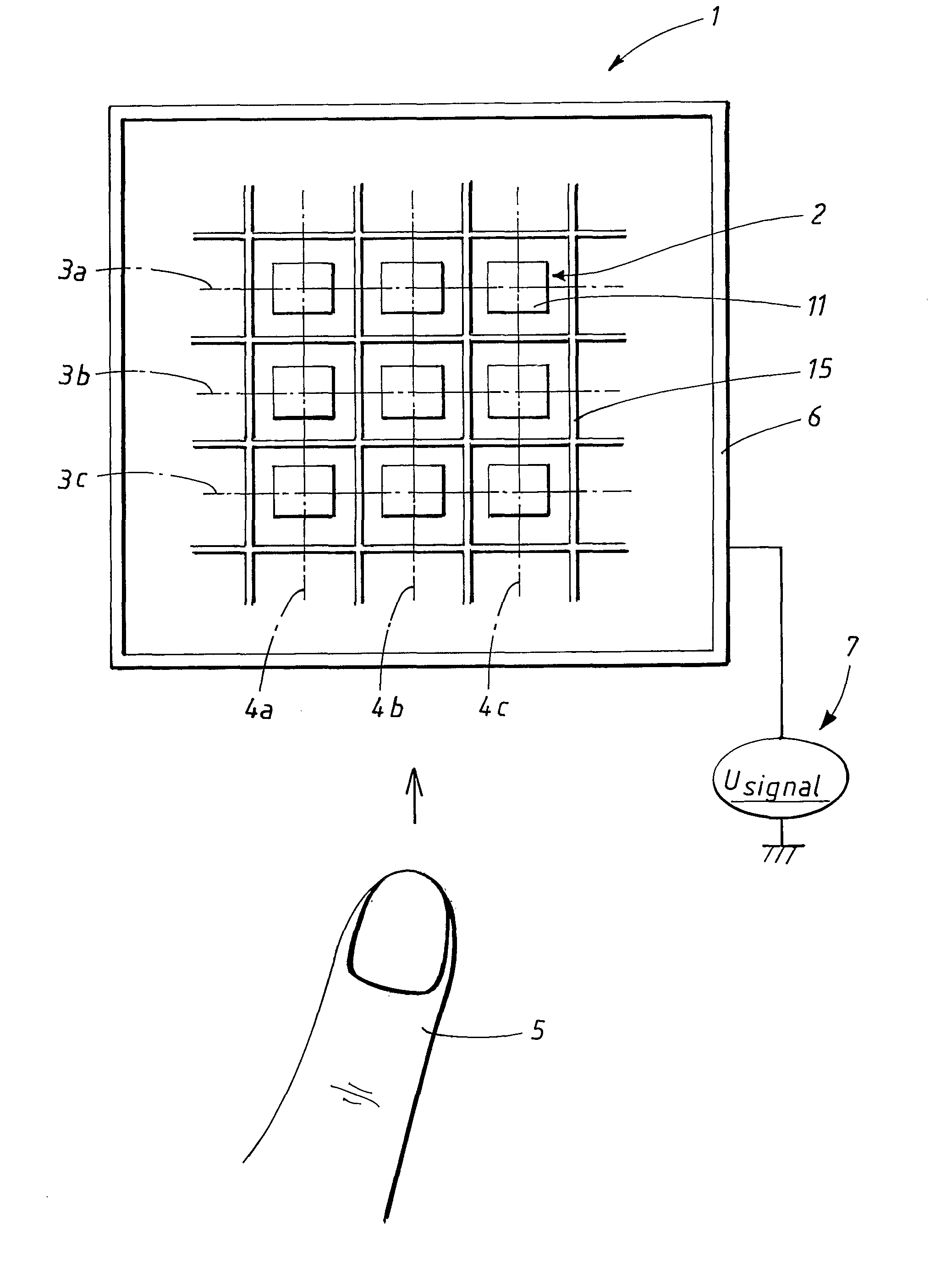
[0071] In the invention, shown in FIG. 6, the control unit 20 of the fingerprint sensor 1 is adapted for injecting a signal Usignal to the finger 5, or sensing a signal from the finger 5, via the sensor electrodes 11. The sensor electrodes 11 alternate, either injecting a signal Usignal or receiving an injected signal via the finger 5. For each sensor element 2, the control unit 20 controls a signal switch 32a that opens and closes a connection from the signal source 7 generating the signal Usignal that is to be injected into the finger 5. Therefore, at a specific moment, some of the sensor electrodes 11 of the fingerprint sensor 1 function as sensor elements while the rest of the sensor electrodes function as means for injecting the signal Usignal to the finger 5. At another moment some of the sensor electrodes 11 may have switched between these functions. In this embodiment, the frame 6 surrounding the fingerprint sensor elements 2 is only needed for ESD protection.
[0072] With reg...
third embodiment
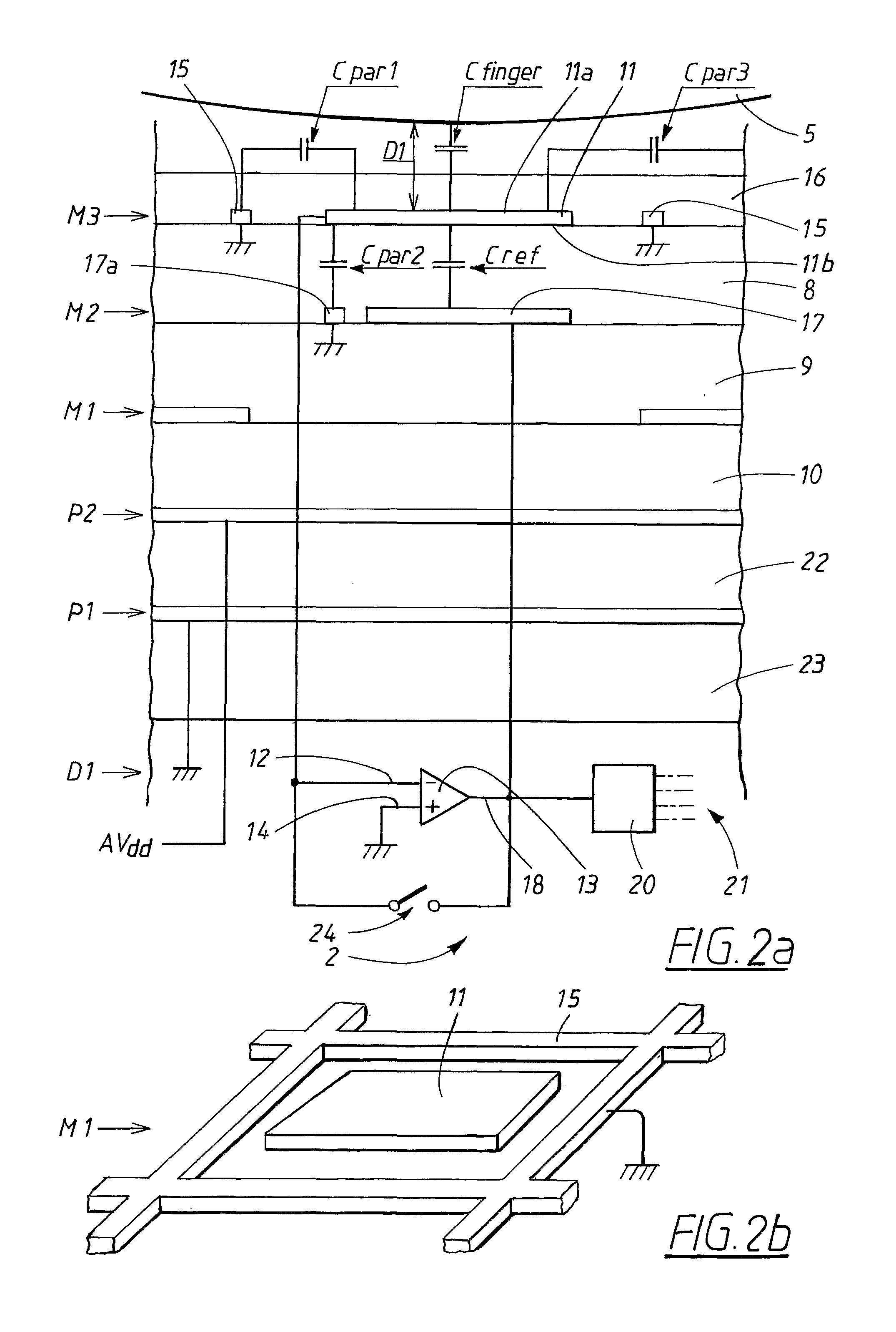
[0077] In FIG. 7, according to the present invention, a fingerprint structure according to the above is used in a different way. The negative input terminal 12 of a charge amplifier is here connected to a sensor electrode 11 in the first conductive layer M3. The fifth layer that is constituted by an electrically conductive layer P1 has a lower electrode 33 formed that is connected to the output 18 of the charge amplifier 13, increasing a distance D2 between the electrodes of the feedback capacitor Cref that now is formed between the sensor 11 electrode and the lower electrode 33, since there are no interfering structures between them, only the intermediate insulting dielectric layers 8, 9, 10, 22. For this purpose, apertures are made in the intermediate conducting layers M1, M2, P2. This increase of D2 decreases the total capacitance at the negative input terminal 12 of the charge amplifier 13, which in turn results in that the total noise of the circuit also decreases, since, as kn...
PUM
 Abstract
Description
Claims
Application Information