Atomic layer deposition apparatus

a technology of atomic layer and apparatus, which is applied in the direction of chemical vapor deposition coating, vacuum evaporation coating, coating, etc., can solve the problems of consuming a lot of time to supply reactant gas having a lower vapor pressure, and affecting the effect of reaction tim

Active Publication Date: 2008-03-20
ASM KOREA LTD
View PDF16 Cites 362 Cited by
  • Summary
  • Abstract
  • Description
  • Claims
  • Application Information

AI Technical Summary

Benefits of technology

[0016]The embodiments described herein provide an ALD apparatus including a lateral flow ALD reaction chamber having advantages of reducing the time required for supplying reactant gases and waste of reactant gases in the case of using a circular substrate having an actual surface area that is much larger than a planar surface would have on a similarly sized substrate.

Problems solved by technology

Accordingly, a gas supply of a constant flux and a constant flow velocity may not be optimal for the substrate with a rough surface having an actual surface area of about fifty times as large as a planar surface on a similar substrate, in that time required for a saturative gas supply cycle may be longer and the amount of gases required for the saturative gas supply cycle may be larger than optimally required.
However, it takes a great deal of time to supply a reactant gas having a lower vapor pressure such as tetrakis(ethylmethylamido)halfnium (TEMAHf) or tetrakis(ethylmethylamido)zirconium (TEMAZr), which are often employed to form a thin film of HfO2 or ZrO2.
In addition, if the reactant gas supplied to the reaction chamber is not used to form a thin film but passes through the reaction chamber, a longer time is required for supplying the reactant gas until completion of saturative adsorption or surface reaction on the whole surface of the substrate.

Method used


Image

  • Atomic layer deposition apparatus
  • Atomic layer deposition apparatus
  • Atomic layer deposition apparatus

Examples


Embodiment Construction

[0033]The present invention will be described more fully hereinafter with reference to the accompanying drawings, in which exemplary embodiments of the invention are shown.

[0034]As those skilled in the art would realize, the described embodiments may be modified in various different ways, all without departing from the spirit or scope of the present invention.

[0035]Now, an exemplary embodiment of the present invention will be described in detail with reference to accompanying drawings.

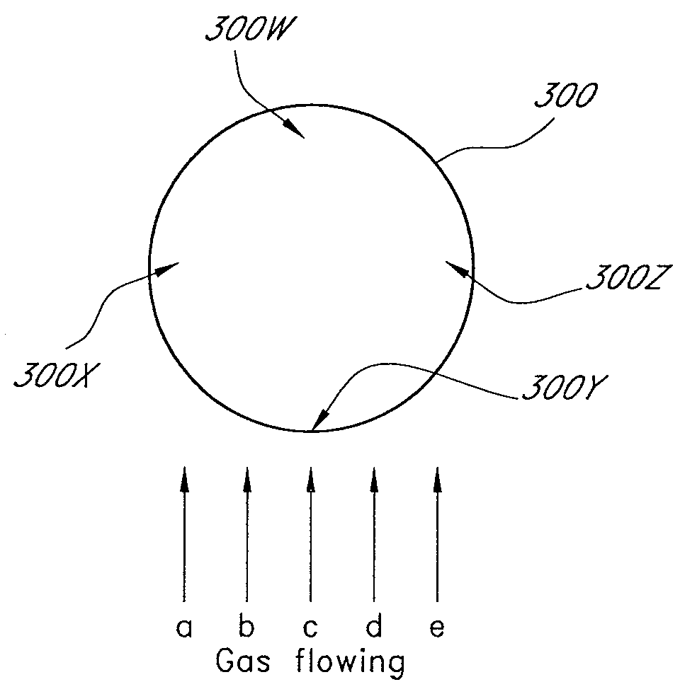
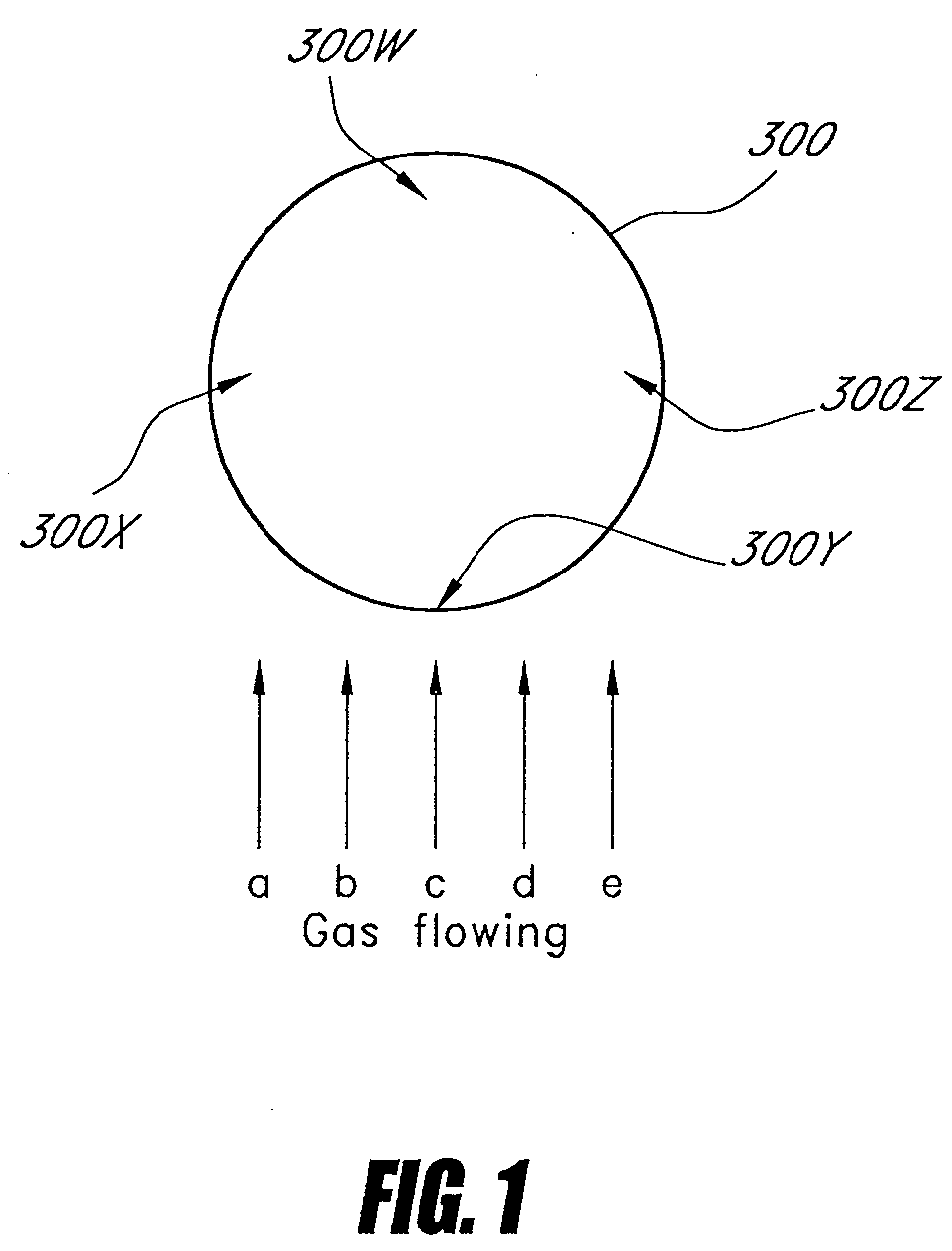
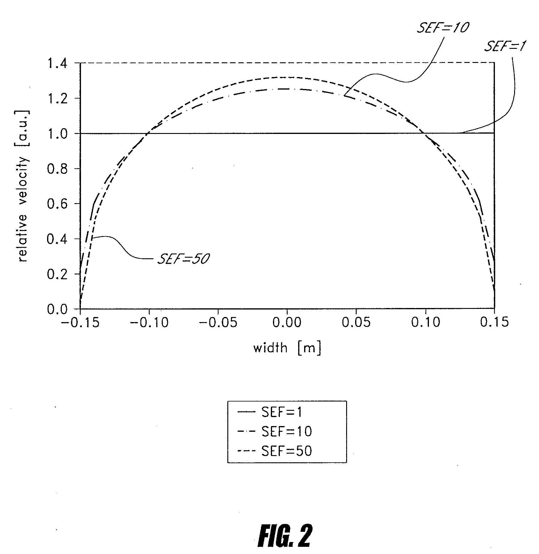
[0036]Firstly, a gas flux on a round substrate having an actual surface area that is different from a planar surface would have on the same substrate will be described with reference to FIG. 2.

[0037]FIG. 2 is a graph representing the most suitable gas velocity for using the minimum quantity of gas in the case of a circular substrate in a lateral flow ALD reaction chamber. In FIG. 2, three cases surface enhancement factor (SEF)=1, SEF=10, and SEF=50 are represented such that the case SEF=1 represents a ...


PUM

PropertyMeasurementUnit
heightaaaaaaaaaa
heightaaaaaaaaaa
heightaaaaaaaaaa

Abstract

The present invention relates to an ALD apparatus, and particularly relates to an ALD apparatus that is suitable for rapidly depositing a thin film on a substrate having an actual area that is larger than a planar substrate. In the reaction chamber of the ALD apparatus according to an exemplary embodiment of the present invention, more gas is supplied to a portion where more gas is required by having differences in the space for gas to flow rather than supplying the gas in a constant flux and a constant flow velocity such that the time required for supplying reactant gases and waste of reactant gases may be minimized to increase productivity of the ALD apparatus. The ceiling of the reaction space is shaped to provide a nonuniform gap over the substrate.

Description

CROSS-REFERENCE TO RELATED APPLICATIONS[0001]This application claims priority to and the benefit of Korean Patent Application No. 10-2006-0091412 filed in the Korean Intellectual Property Office on Sep. 20, 2006, the entire disclosure of which is incorporated herein by reference.BACKGROUND OF THE INVENTION[0002]1. Field of the Invention[0003]The present invention relates to an atomic layer deposition (ALD) apparatus, and particularly relates to an ALD apparatus that is suitable for rapidly depositing a thin film on a structure having a larger actual area than an apparent area, such as DRAM.[0004]2. Description of the Related Art[0005]In the manufacture of semiconductor devices, efforts for improving apparatuses and processes to be suitable for forming a high quality thin film on a substrate have continued. In ALD methods, separate pulses of at least two reactants are sequentially introduced on the substrate, a surface reaction of the reactants occurs to form a monolayer on the surfa...

Claims


Application Information

Patent Timeline
Patent Type & Authority Applications(United States)
IPC IPC(8): C23C16/00
CPCC23C16/045C23C16/45544C23C16/45508H01L21/20
Inventor HONG, KYUNG ILKIM, DAE YOUNPARK, HYUNG-SANGJEONG, SANG JINKOH, WONYONGTERHORST, HERBERT
Owner ASM KOREA LTD
Why Eureka
Try Eureka