Semiconductor device and method of manufacturing the same

a technology of semiconductors and dielectric films, applied in the direction of semiconductor devices, electrical equipment, transistors, etc., can solve the problems of increasing leakage, difficulty in achieving a desired threshold voltage vth, etc., and achieve the effect of enhancing channel length, and enhancing the reliability of gate dielectric films

Active Publication Date: 2008-03-27
MICRON TECH INC
View PDF21 Cites 16 Cited by
  • Summary
  • Abstract
  • Description
  • Claims
  • Application Information

AI Technical Summary

Benefits of technology

[0027]In accordance with the above-mentioned semiconductor device, since a cross-sectional surface contour of the trench is substantially U-shaped and a surface extending from the opening portion to the bottom portion is configured with a curved surface, a shape protruding at an acute angle is not formed in the gate dielectric film even when the gate oxide film is formed in the trench. Accordingly, the reliability of the gate dielectric film can be enhanced because there is not a possibility that leakage is increased due to the electric field concentrated to the gate dielectric film.
[0028]Since the width of the opening portion of the trench is smaller than that of the bottom portion of the trench, the trench has a shape narrowed in the opening portion. Therefore, the channel length can further increase, and a desired threshold voltage Vth can be achieved even when a wiring of the semiconductor device is miniaturized.
[0029]Since a ridge line portion is not interposed on a surface extending from the opening portion to the bottom portion, a shape protruding at an acute angle is not formed in the gate dielectric film. Therefore, a risk of increasing leakage due to an electric field concentrated to the gate dielectric film is avoided, and the reliability of the gate dielectric film can be further enhanced.
[0030]In a process of forming a trench in accordance with a method of manufacturing the above-mentioned semiconductor device, the trench whose inner surface is a smooth curved surface is formed by performing a sacrifice oxidation treatment and an oxide film removing treatment after high-temperature hydrogen anneal. Accordingly, a shape protruding at an acute angle is not formed in a gate dielectric film even when the gate dielectric film is formed in the trench. For this reason, a risk of increasing leakage due to the electric field concentrated to the gate dielectric film is avoided, so that the reliability of the gate dielectric film can further increase.
[0031]Since the sacrifice oxidation treatment is performed in an atmosphere including organic halide gas, the whole of an inner surface of the formed trench becomes almost a smooth curved surface. As a result, the reliability of the gate dielectric film can further increase because a shape protruding at an acute angle is not formed in the gate dielectric film.
[0032]Since a region where an oxide film is formed extends to an outer side of a first recess portion by forming the oxide film in the first recess portion by means of a thermal oxidation method, the oxide film remains in the first recess portion while the oxide film is etched when a second recess portion is formed. Therefore, the shape of the first recess portion can be retained until just before the sacrifice oxidation treatment. Accordingly, a trench having a shape in which the width of an opening portion is narrowed can be formed, and thus a semiconductor device whose channel length is sufficiently secured can be manufactured.

Problems solved by technology

However, it is difficult to achieve a desired threshold voltage Vth even in such a trench embedded semiconductor device when a wiring is further miniaturized.
As a result, an electric field is concentrated to the gate dielectric film 206 of the boundary portion, thereby increasing leakage.

Method used


Image

  • Semiconductor device and method of manufacturing the same
  • Semiconductor device and method of manufacturing the same
  • Semiconductor device and method of manufacturing the same

Examples


Embodiment Construction

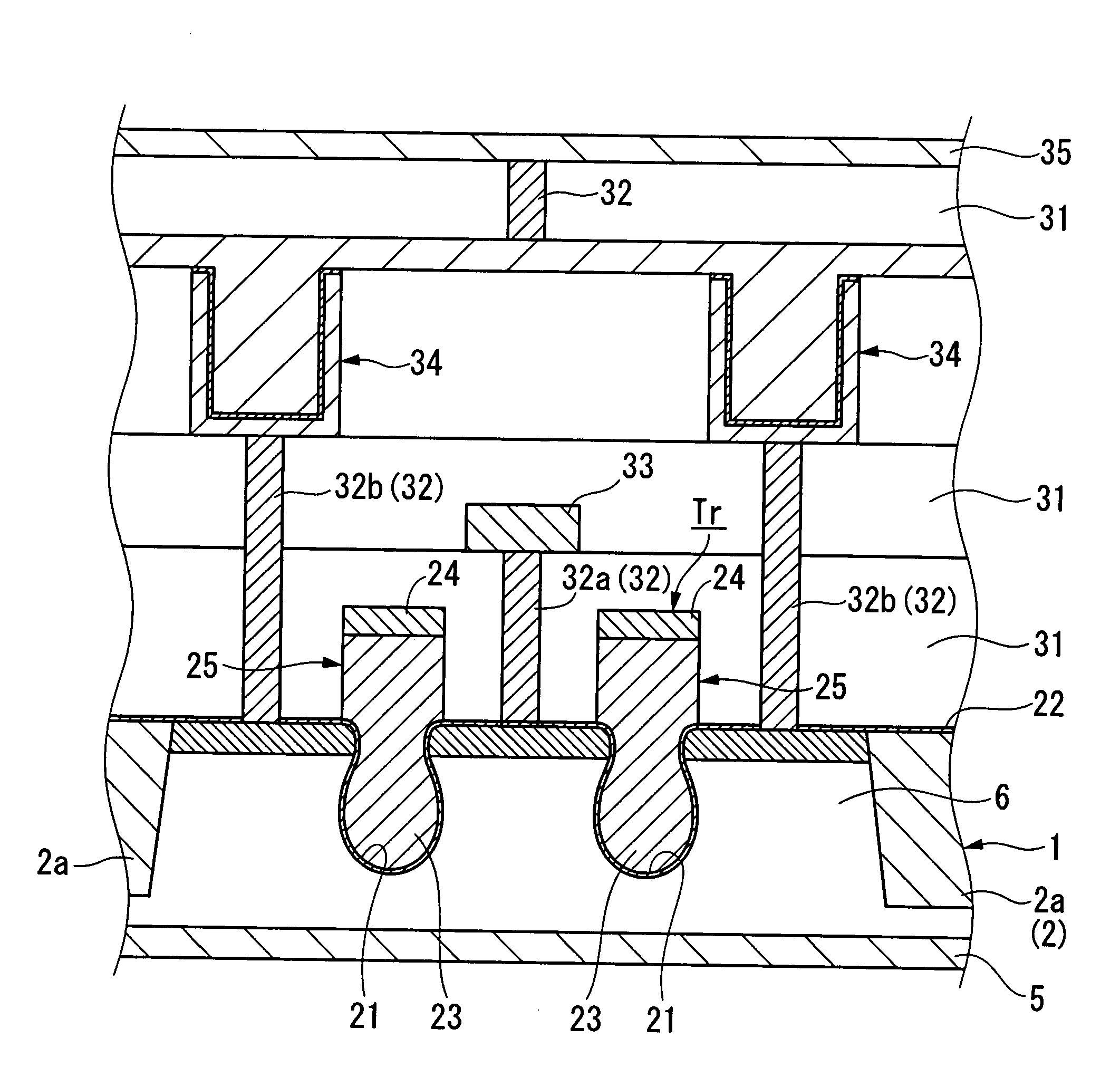
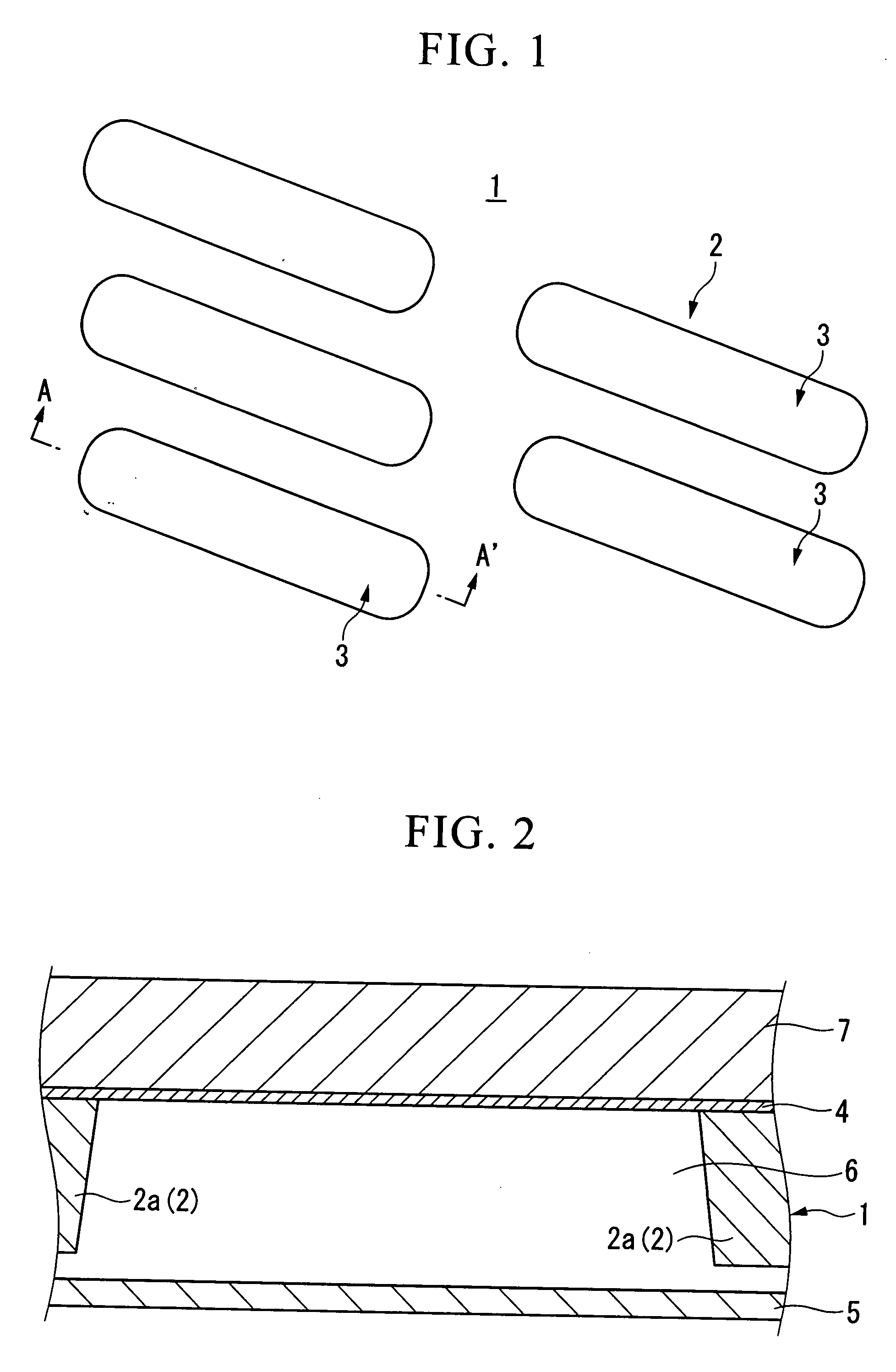
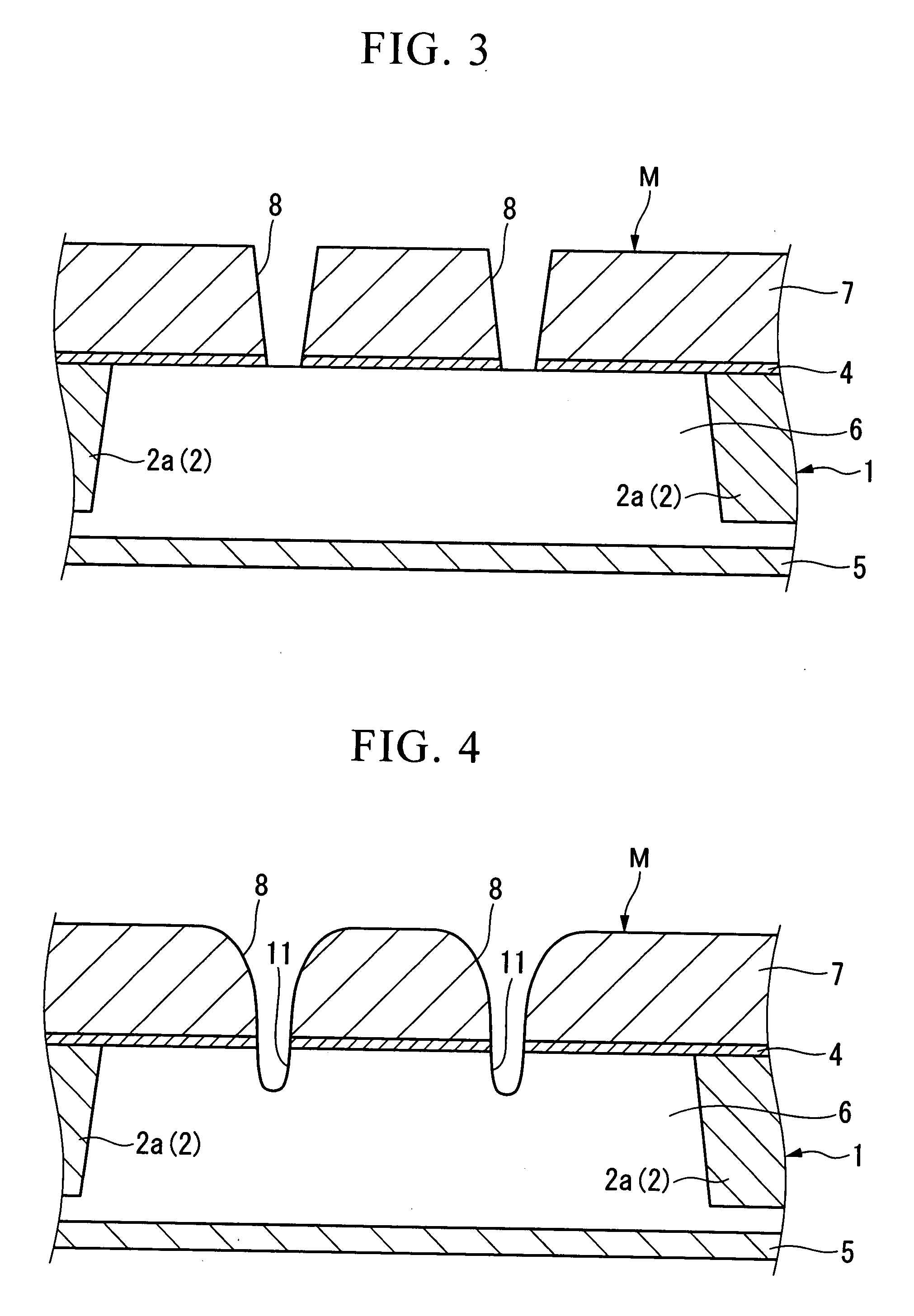
[0047]Hereinafter, a semiconductor device and a method of manufacturing the same will be described with the accompanying drawings. It is to be noted that the drawings to be referenced in the following description are for explaining the semiconductor device and the method of manufacturing the same in accordance with an embodiment of the present invention, and thus the size, thickness, and dimension of each part shown in the respective drawings may be different from those of an actual part in the semiconductor device and the method of manufacturing the same.

Method of Manufacturing Semiconductor Device

[0048]FIGS. 1 to 14 are process views for explaining a method of manufacturing a semiconductor device in accordance with the present embodiment. The method of manufacturing a semiconductor device in accordance with the present embodiment is mainly configured from a process of forming a trench in a semiconductor substrate (trench forming process), a process of forming a gate dielectric fil...


PUM


Abstract

A semiconductor device in which the reliability of a gate dielectric film is high and a channel length is sufficiently secured and a method of manufacturing the same are provided. The semiconductor device comprises a trench gate transistor. The trench gate transistor comprises: a trench provided in a semiconductor substrate; a gate electrode formed in the trench through a gate dielectric film; and a diffusion layer formed in the vicinity of the trench. The trench comprises: an opening portion provided in a surface of the semiconductor substrate; a recess curved surface portion whose cross-sectional contour is a substantially circular arc shape; and a connection curved surface portion connecting the recess curved surface portion and the opening portion. The connection curved surface portion and the recess curved surface portion are integrated in a continuous curved surface without interposing a ridge line portion therebetween.

Description

BACKGROUND OF THE INVENTION[0001]1. Field of the Invention[0002]The present invention relates to a semiconductor device and a method of manufacturing the same.[0003]Priority is claimed on Japanese Patent Application No. 2006-257021, filed Sep. 22, 2006 and Japanese Patent Application No. 2007-217162, filed Aug. 23, 2007, the contents of which are incorporated herein by reference.[0004]2. Description of the Related Art[0005]Semiconductor devices are known in which an n-type diffusion layer, a gate dielectric film, and a gate electrode are formed on a surface of a semiconductor substrate. FIG. 16 is a schematic cross-sectional view showing a cross-sectional structure of a conventional semiconductor device provided with a gate electrode embedded in a trench. In a semiconductor device 101 shown in FIG. 16, a transistor structure T is formed between a pair of trench isolation sections 102. Specifically, an n-type diffusion layer 104 having a source region and a drain region is formed on ...

Claims


Application Information

Patent Timeline
Patent Type & Authority Applications(United States)
IPC IPC(8): H01L29/78H01L21/3205H01L21/336H01L21/8242H01L27/108H01L29/40H01L29/41H01L29/423H01L29/49
CPCH01L27/10814H01L27/10823H01L27/10876H01L29/78H01L29/66553H01L29/66621H01L29/1037H10B12/34H10B12/315H10B12/053
Inventor FUJIMOTO, HIROYUKIUEDA, YASUHIKO
Owner MICRON TECH INC
Why Eureka
Try Eureka