Signal transfer circuit, display data processing apparatus, and display apparatus

a signal transfer and data processing technology, applied in the field of signal transfer circuits, can solve problems such as difficult to increase operating frequency, electromagnetic interference deterioration, etc., and achieve the effect of reducing voltage variation

Inactive Publication Date: 2008-04-03
PANASONIC CORP
View PDF12 Cites 3 Cited by
  • Summary
  • Abstract
  • Description
  • Claims
  • Application Information

AI Technical Summary

Benefits of technology

[0015] In the signal transfer circuit, when the polarity of the signal input to the input node is transitioned, the second input / output circuit performs an operation reverse to that of the first input / output circuit. Thus, charging and discharging of the load capacitance are shared by the first and second input / output circuits, thereby making it possible to reduce a voltage variation of each of the first and power supply wirings.

Problems solved by technology

Therefore, the amount of a variation in voltage of the power supply wiring which occurs due to charging or discharging of the buffer circuit increases, leading to a deterioration in ElectroMagnetic Interference (EMI).
Also, since the voltage variation amount of the power supply wiring is large, it is difficult to increase the operating frequency.

Method used


Image

  • Signal transfer circuit, display data processing apparatus, and display apparatus
  • Signal transfer circuit, display data processing apparatus, and display apparatus
  • Signal transfer circuit, display data processing apparatus, and display apparatus

Examples


first embodiment

Variation of First Embodiment

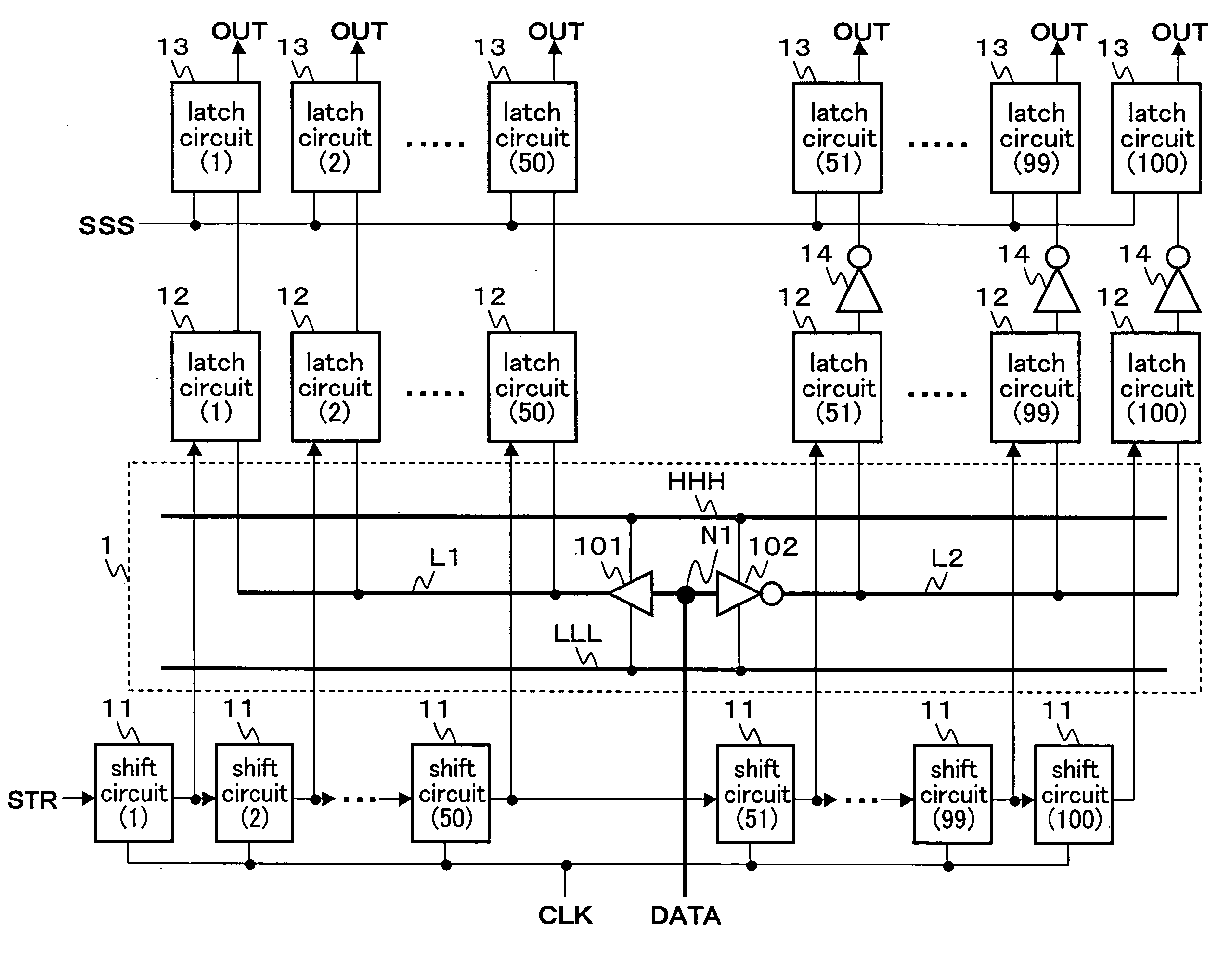
[0047] As shown in FIG. 4, the signal transfer circuit 1 may further comprise inverter circuits 103 and 104. The inverter circuit 103 is provided for the signal wiring L1, while the inverter circuit 104 is provided for the signal wiring L2. Note that it is here assumed that the 26th-stage to 50th-stage latch circuits 12 are connected to the signal wiring L1 between the buffer circuit 101 and the inverter circuit 103, while the 51st-stage to 75th-stage latch circuits 12 are connected to the signal wiring L2 between the inverter circuits 102 and 104. Also, in order to bring the display data signal DATA inverted by the inverter circuit 103 back to the original polarity, an inverter circuit 14 is provided for each of the first-stage to 25th-stage latch circuits 12. On the other hand, since the display data signal DATA inverted by the inverter circuit 102 is brought back to the original polarity by the inverter circuit 104, the inverter circuit 14 is not prov...

second embodiment

[0055]FIG. 6 shows a configuration of a signal transfer circuit according to a second embodiment of the present invention. This signal transfer circuit 2 comprises a buffer circuit 201 instead of the inverter circuit 102 of FIG. 4. Also, a display data signal DATA output from the buffer circuit 201 is not inverted, so that the inverter circuit 14 is not provided for any of the 51st-stage to 75th-stage latch circuits 12. On the other hand, in order to bring the display data signal DATA inverted by the inverter circuit 104 back to the original polarity, the inverter circuit 14 is provided for each of the 76th-stage to 100th-stage latch circuits 12. The other portions are similar to those of FIG. 4.

[0056] Next, an operation of the signal transfer circuit 2 of FIG. 6 will be described with reference to FIG. 7.

[0057] When the display data signal DATA goes from the low level to the high level, an output S201 of the buffer circuit 201 goes from the low level to the high level, so that th...

third embodiment

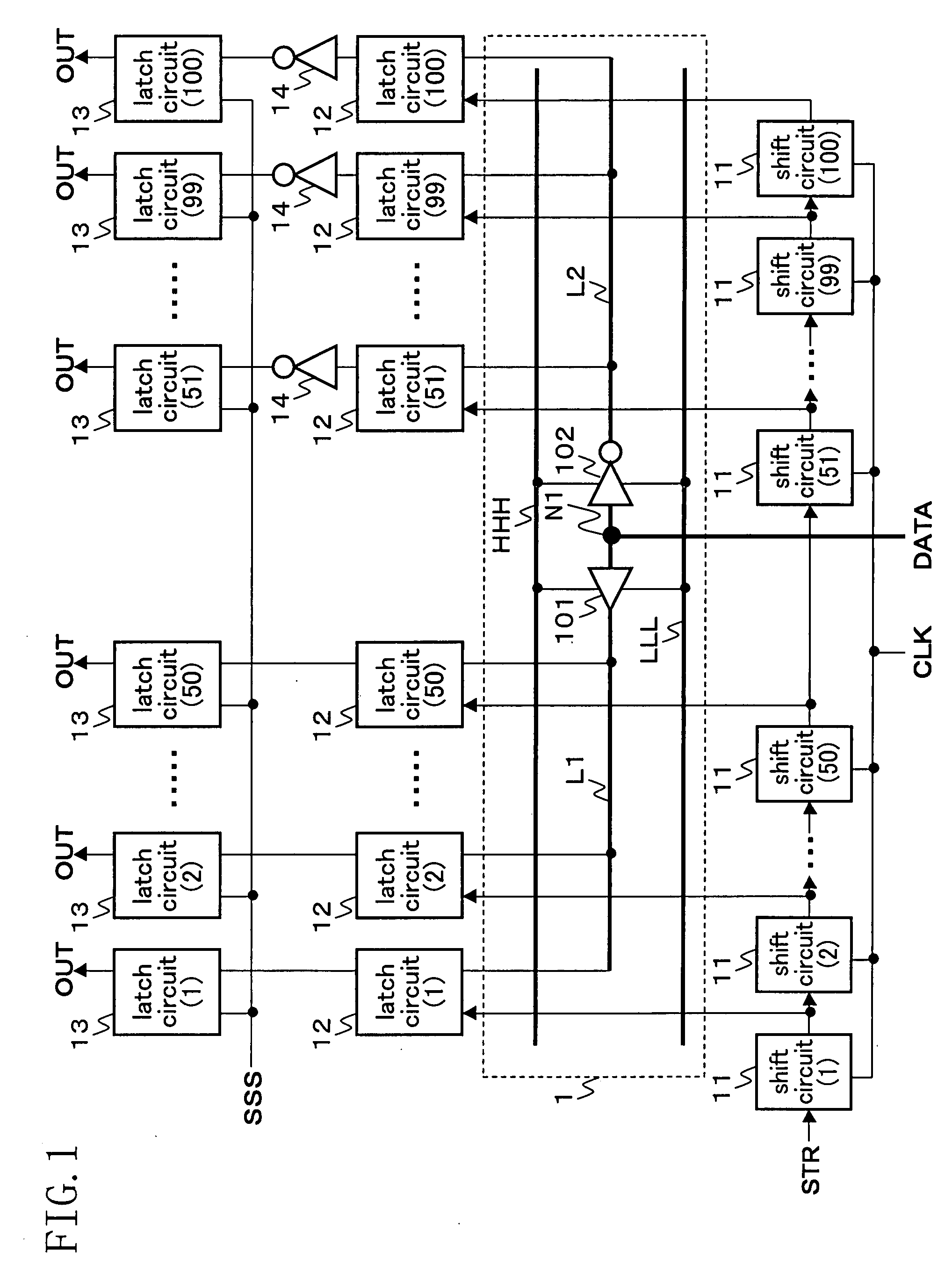
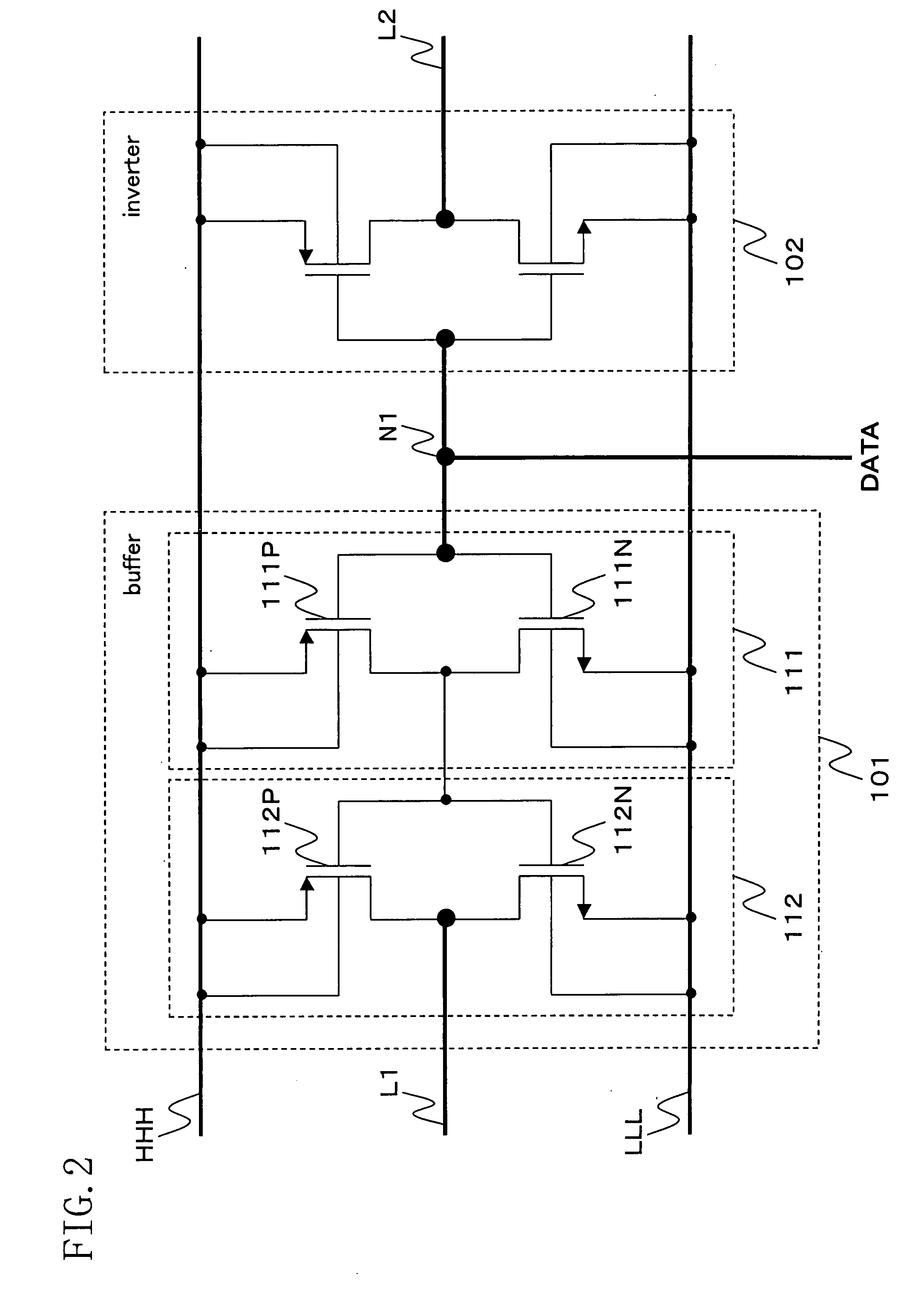
[0062]FIG. 9 shows a configuration of a signal transfer circuit according to a third embodiment of the present invention. This signal transfer circuit 3 comprises a buffer circuit 301, a signal wiring L3, and an inverter circuit 302. An input terminal of the buffer circuit 301 is connected to an input node N1. The signal wiring L3 extends from an output terminal of the buffer circuit 301. The inverter circuit 302 is provided for the signal wiring L3. The other portions are similar to those of FIG. 1.

[0063] Next, an operation of the signal transfer circuit 3 of FIG. 9 will be described with reference to FIG. 10.

[0064] When the polarity of the display data signal DATA is transitioned, the inverter circuit 302 starts an operation reverse to the buffer circuit 301 with a delay from a charging or discharging operation performed by the buffer circuit 301. Thereby, an output S301 of the buffer circuit 301 is transitioned, and thereafter, an output S302 of the inverter circuit 302 is tran...


PUM


Abstract

First and second input/output circuits each have an input terminal connected to the input node. A first power supply wiring supplies a first voltage. A second power supply wiring supplies a second voltage. The first and second input/output circuits each select any one of the first and second power supply wirings, depending on the polarity of an input signal, to output an output signal. The first and second input/output circuits each have any one of a first characteristic in which an output signal having the same polarity as that of the input signal is output and a second characteristic in which an output signal having a polarity opposite to that of the input signal is output. The characteristics possessed by the first and second input/output circuits are different from each other.

Description

BACKGROUND OF THE INVENTION [0001] 1. Field of the Invention [0002] The present invention relates to a circuit for transferring a signal, and a display data processing apparatus and a display apparatus comprising the signal transfer circuit. [0003] 2. Description of the Related Art [0004] Conventionally, a buffer circuit is provided for a signal wiring connecting circuits so as to accurately transfer the logic level of a signal between the circuits or prevent backflow of a current. The buffer circuit is connected to a high-level power supply wiring and a low-level power supply wiring. A signal to be transferred is input to an input terminal of the buffer circuit. Also, a circuit to which the signal is to be transferred is connected to a signal wiring extending from an output terminal of the buffer circuit. For example, in a display panel driving apparatus, a display data signal is input to the input terminal of the buffer circuit while a plurality of stages of latch circuits for lat...

Claims


Application Information

Patent Timeline
Patent Type & Authority Applications(United States)
IPC IPC(8): G06F3/038
CPCG09G2310/0264G09G2310/0291G09G2310/0286G09G3/20
Inventor MATSUMOTO, KAZUYAIITSUKA, JUNHAMAHASHI, YOSHIHISAISHIKAWA, TOMOYA
Owner PANASONIC CORP
Why Eureka
Try Eureka