SiGe selective growth without a hard mask

a selective growth and hard mask technology, applied in the field of semiconductor devices, can solve the problems of significant process integration issues, affecting the band alignment and charge transport properties of semiconductors, and complicating an already complex process

Inactive Publication Date: 2008-04-10
TAIWAN SEMICON MFG CO LTD
View PDF9 Cites 188 Cited by
  • Summary
  • Abstract
  • Description
  • Claims
  • Application Information

AI Technical Summary

Benefits of technology

[0006]These and other problems are generally reduced, solved or circumvented, and technical advantages are generally achieved, by embodiments of the present invention, which provides

Problems solved by technology

Stress distorts or strains the semiconductor crystal lattice, which affects the band alignment and charge transport properties of the semiconductor.
A problem with the prior art is that the new materials and methods required of strain-e

Method used


Image

  • SiGe selective growth without a hard mask
  • SiGe selective growth without a hard mask
  • SiGe selective growth without a hard mask

Examples


Embodiment Construction

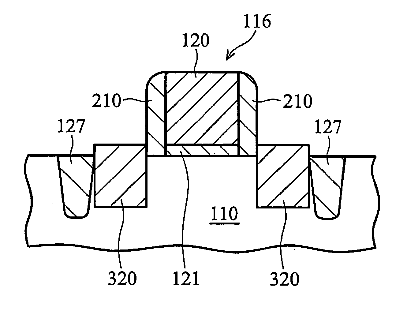
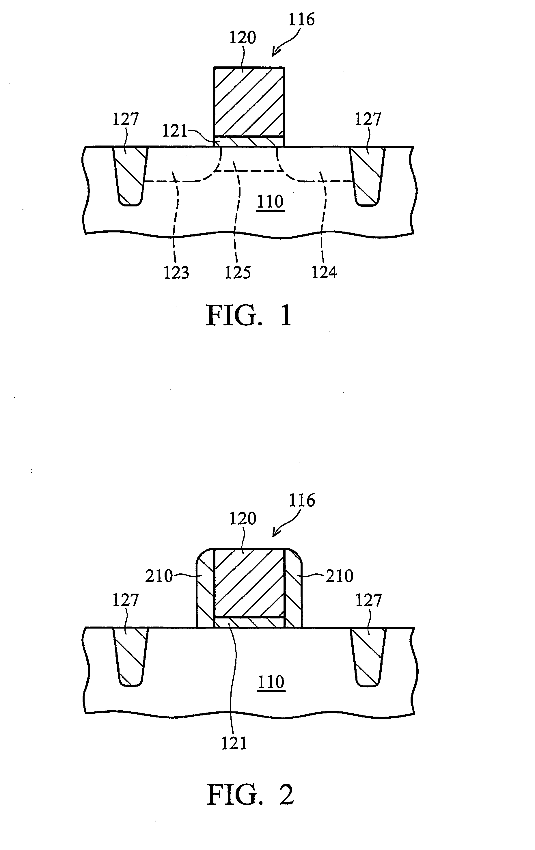
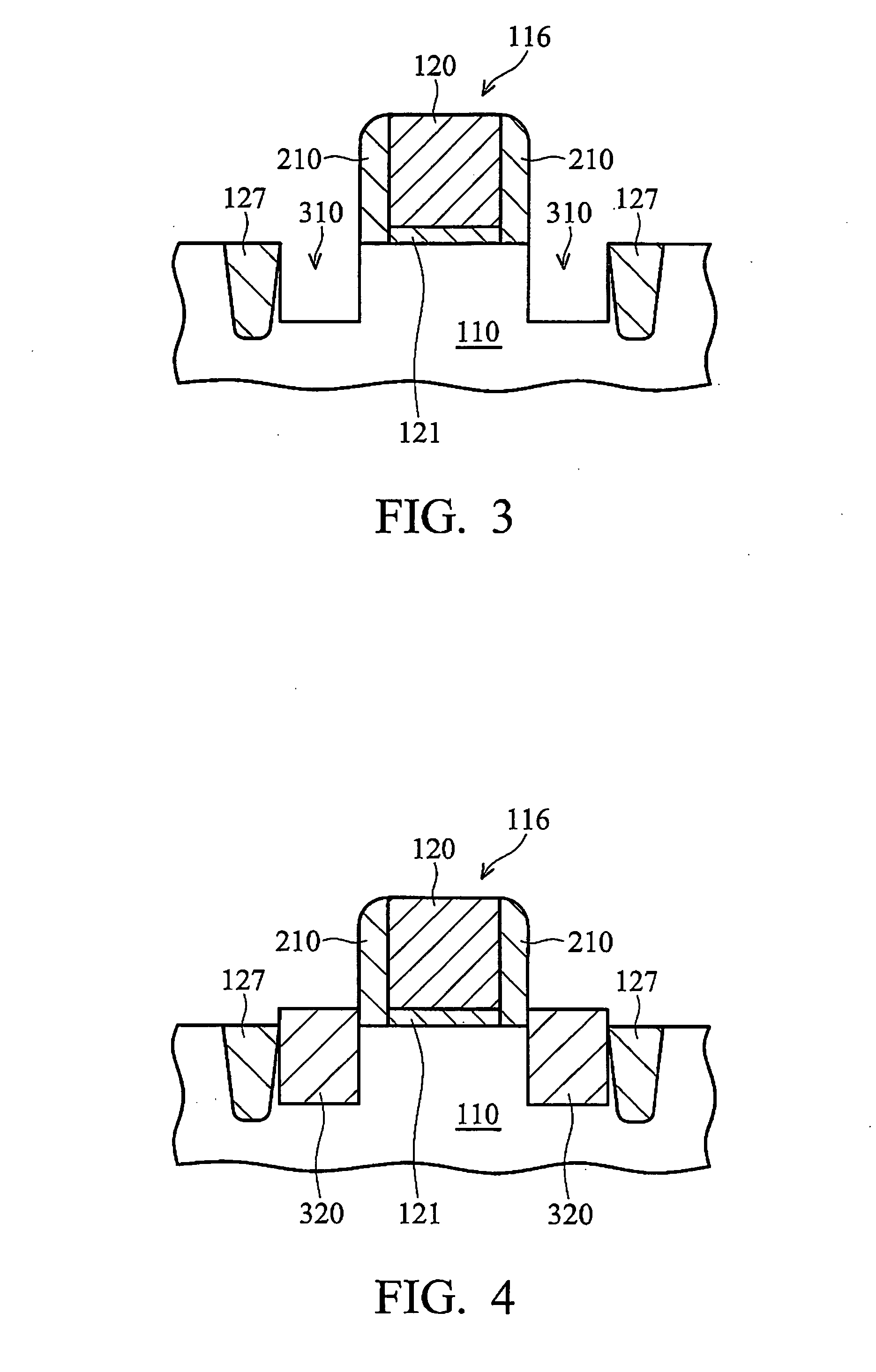
[0015]The making and using of the presently preferred embodiments are discussed in detail below. It should be appreciated, however, that the present invention provides many applicable inventive concepts that can be embodied in a wide variety of specific contexts. The specific embodiments discussed are merely illustrative of specific ways to make and use the invention, and do not limit the scope of the invention. The intermediated stages of manufacturing a preferred embodiment of the present invention are illustrated. Throughout the various views and illustrative embodiments of the present invention.

[0016]This invention relates generally to semiconductor device fabrication and more particularly to structures and methods for strained transistors. This invention will now be described with respect to preferred embodiments in a specific context, namely the creation of a MOSFET device. It is believed that embodiments of this invention are particularly advantageous when used in this proces...


PUM


Abstract

MOS transistors having localized stressors for improving carrier mobility are provided. Embodiments of the invention comprise a gate electrode formed over a substrate, a carrier channel region in the substrate under the gate electrode, and source/drain regions on either side of the carrier channel region. The source/drain regions include an embedded stressor having a lattice spacing different from the substrate. In a preferred embodiment, the substrate is silicon and the embedded stressor is SiGe or SiC. An epitaxy process that includes using HCl gas selectively forms a stressor layer within the crystalline source/drain regions and not on polycrystalline regions of the structure. A preferred epitaxy process dispenses with the source/drain hard mask required of conventional methods. The embedded SiGe stressor applies a compressive strain to a transistor channel region. In another embodiment, the embedded stressor comprises SiC, and it applies a tensile strain to the transistor channel region.

Description

TECHNICAL FIELD[0001]This invention relates generally to semiconductor devices, and more particularly to methods and structures for introducing stress into semiconductor devices in order to improve charge carrier mobility.BACKGROUND[0002]The continued development of metal-oxide-semiconductor field-effect transistors (MOSFET) has improved the speed, density, and cost per unit function of integrated circuits. One way to improve transistor performance is through selective application of stress to the transistor channel region. Stress distorts or strains the semiconductor crystal lattice, which affects the band alignment and charge transport properties of the semiconductor. By controlling the magnitude and distribution of stress in a finished device, manufacturers can increase carrier mobility and improve device performance. There are several existing approaches of introducing stress in the transistor channel region.[0003]One conventional approach includes forming an epitaxial, strained...

Claims


Application Information

Patent Timeline
IPC IPC(8): H01L21/8234
CPCH01L21/02381H01L21/02529H01L21/02532H01L21/0262H01L29/7848H01L29/165H01L29/66628H01L29/66636H01L21/02639
Inventor LIN, HSIEN-HSINLIN, LI-TE S.LEE, TZE-LIANGYU, MING-HUA
Owner TAIWAN SEMICON MFG CO LTD
Why Eureka
Try Eureka