Silicon strain engineering accomplished via use of specific shallow trench isolation fill materials

a technology of filling material and silicon strain, which is applied in the direction of semiconductor devices, basic electric elements, electrical equipment, etc., can solve the problems of significant cost and process complexity in the process sequence of devices used to fabricate mosfet devices, and achieve the effects of improving the performance of mosfet and vertical bipolar devices, improving performance, and improving performan

Inactive Publication Date: 2006-07-25
TAIWAN SEMICON MFG CO LTD
View PDF13 Cites 51 Cited by
  • Summary
  • Abstract
  • Description
  • Claims
  • Application Information

AI Technical Summary

Benefits of technology

[0010]It is still yet another object of this invention to form vertical bipolar transistor with enhanced performance via a base region under biaxial strain induced by an adjacent TI region, filled with a dielectric layer comprised with either a higher or lower α, than silicon.
[0011]In accordance with the present invention a method of improving the performance of MOSFET and vertical bipolar devices, via creation of a strained silicon region used as the channel region of the MOSFET device, and used as the base region of the vertical bipolar device, wherein the strained silicon regions is formed via a mis-match to adjacently located TI regions filled with dielectric layer comprised with either a higher or lower α, than silicon, has been developed. A first embodiment of this invention entails the formation of TI regions for MOSFET devices wherein the TI region of a P type MOSFET device is comprised with a dielectric layer with a lower α than silicon, creating a compressively strained silicon layer located between TI regions, and wherein the TI region of an N type MOSFET device is comprised with a dielectric layer with a higher α than silicon, creating a silicon layer featuring a tensile strain, located between TI regions. Growth of a gate insulator layer on the strained silicon layer, formation of an overlying gate structure on the gate insulator layer, and formation of source / drain regions in portions of the strained silicon layer not covered by the gate structure, result in a MOSFET device comprised with a channel region formed in the strained silicon layer.
[0012]A second embodiment of this invention again entails the formation of TI regions comprised with dielectric fills featuring either a higher α, (for vertical PNP devices), or a lower α, (for vertical NPN devices), than the thermal expansion coefficient than silicon, wherein a strained silicon region is induced in the portion of semiconductor substrate located between TI regions. A well region, of an opposite conductivity type than that of the semiconductor substrate, is formed in the region of the semiconductor substrate located between the TI regions. A top portion of the well region is than doped to a conductivity type opposite to the conductivity type of the well region, forming a vertical PNP, or vertical NPN bipolar device, in which the base region, or uncompensated well region, is located in the strained silicon region. The enhancement of carriers in the strained silicon, base region results in a performance increase for the vertical bipolar devices when compared to counterpart vertical bipolar devices formed in non-strained silicon regions.

Problems solved by technology

However the above approach requires the growth of the semiconductor alloy layer, followed by the epitaxial growth of the strained silicon layer, both adding significant cost and process complexity to the device process sequences used to fabricate MOSFET devices.

Method used


Image

  • Silicon strain engineering accomplished via use of specific shallow trench isolation fill materials
  • Silicon strain engineering accomplished via use of specific shallow trench isolation fill materials
  • Silicon strain engineering accomplished via use of specific shallow trench isolation fill materials

Examples


Embodiment Construction

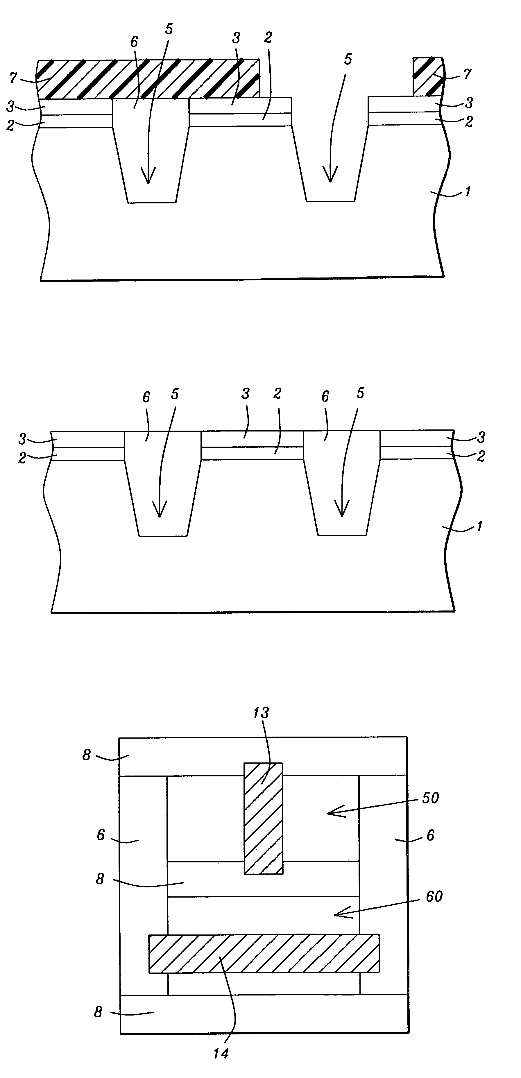
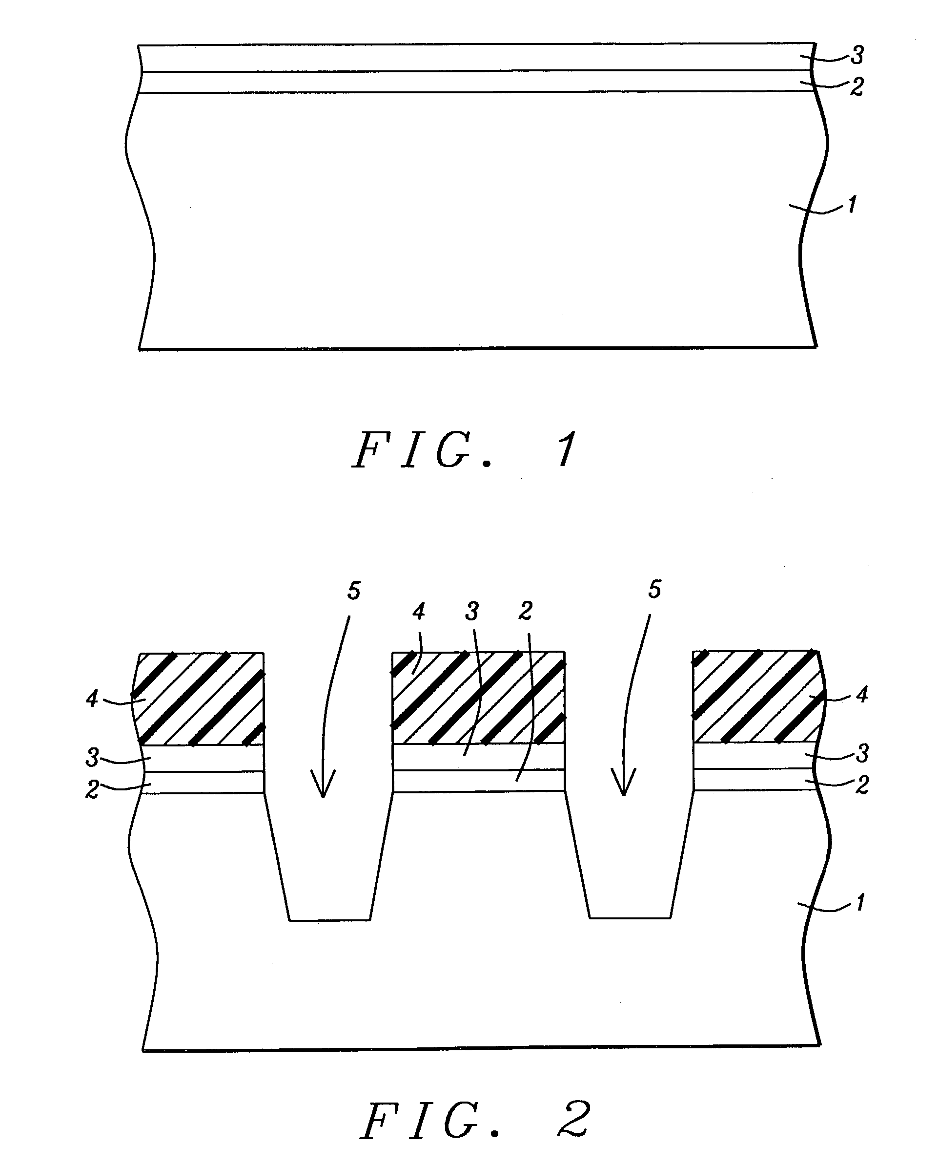
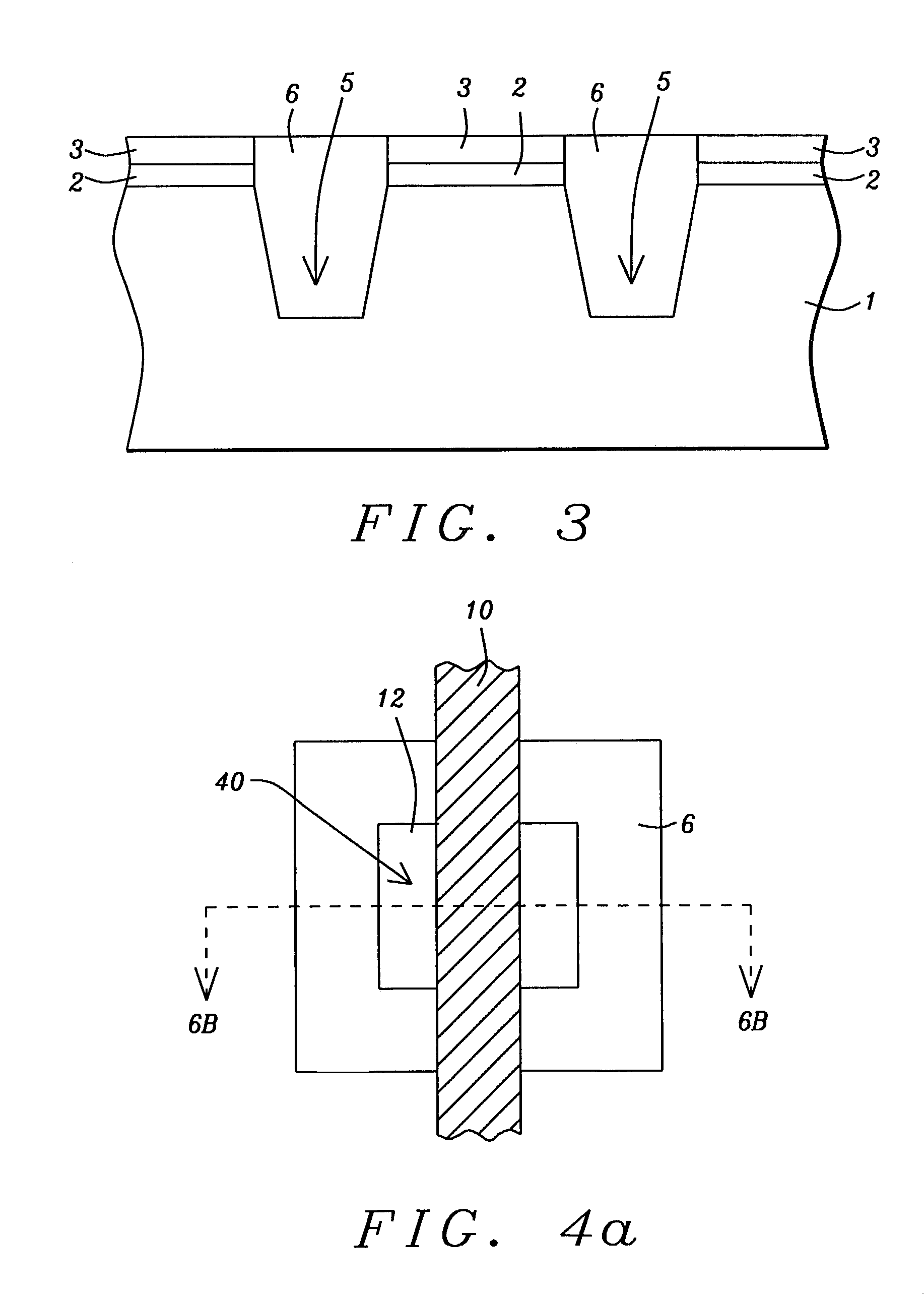
[0016]The method of forming MOSFET devices featuring channel regions formed in strained silicon layers, as well as the method of fabricating vertical bipolar devices featuring base regions formed in a strained silicon regions, will now be described in detail. These methods based on current 0.13 um CMOS generation technology can be extended to future 90 nm generation and beyond. A first embodiment of this invention is directed at the fabrication of MOSFET devices in which the channel region of both P channel, (PMOS), and N channel (NMOS), devices are located in strained silicon layers, which in turn are formed via a material mis-match between silicon and the dielectric material used to fill adjacently located TI regions. A P type semiconductor substrate 1, comprised of single crystalline silicon featuring a crystallographic orientation, is used and schematically shown in FIG. 1. Silicon oxide layer 2, to be used as a pad oxide layer, is typically grown via thermal oxidation procedur...


PUM


Abstract

A method of forming a strained silicon layer created via a material mis-match with adjacent trench isolation (TI), regions filled with a dielectric layer comprised with either a higher, or lower thermal expansion coefficient than that of silicon, has been developed. Filling of trenches with a dielectric layer comprised with a higher thermal expansion coefficient than that of silicon results in a tensile strain in planar direction and compressive strain in vertical direction, in an adjacent silicon region. Enhanced electron mobility in channel regions of an N channel MOSFET device, and enhanced hole mobility and transit time in an N type base region of a vertical PNP bipolar device, is realized when these elements are formed in the silicon layer under tensile strain. Filling of trenches with a dielectric layer comprised with a lower thermal expansion coefficient than the thermal expansion coefficient of silicon results in a compressive strain in planar directions and tensile strain in vertical directions, in an adjacent silicon region. Enhanced hole mobility in channel regions of an P channel MOSFET device, and enhanced electron mobility and transit time in a P type base region of a vertical NPN bipolar device, is realized when these elements are formed in the silicon layer under compressive strain.

Description

BACKGROUND OF THE INVENTION[0001](1) Field of the Invention[0002]The present invention relates to methods used to fabricate semiconductor devices, and more specifically to a method used to increase the performance of metal oxide semiconductor field effect transistor (MOSFET), and of vertical bipolar devices, via use of specific trench isolation (TI), fill materials.[0003](2) Description of Prior Art[0004]Formation of strained, silicon channel regions in MOSFET devices, can enhance carrier transport properties and thus improve device performance for MOSFET devices. Various approaches have been applied in attempts to introduce strain in a MOSFET channel region. Channel regions with the desired strain have been obtained in strained silicon layers, when the silicon layer is grown overlying relaxed semiconductor alloy layers such as silicon-germanium, or silicon-germanium-carbon. However the above approach requires the growth of the semiconductor alloy layer, followed by the epitaxial gr...

Claims


Application Information

Patent Timeline
Patent Type & Authority Patents(United States)
IPC IPC(8): H01L21/76H01L21/762H01L21/8238H01L29/732H01L29/78
CPCH01L21/76229H01L21/823807H01L29/7842H01L29/732H01L29/78H01L21/823878
Inventor CHI, MIN-HWAYEO, YEE-CHIAHU, CHENMING
Owner TAIWAN SEMICON MFG CO LTD
Why Eureka
Try Eureka