Bondable conductive ink

a technology of conductive ink and flexible type, applied in the field of flexible type circuit assembly, can solve the problems of low cost of flexible printed circuit assembly, relatively costly, and inability to easily connect and connect with and to other circuit assembly, devices,/or apparatuses, etc., and achieve cost-effective attachment and/or interconnection, reliable

Inactive Publication Date: 2008-04-17
DOUGLAS JOEL S MR
View PDF1 Cites 76 Cited by
  • Summary
  • Abstract
  • Description
  • Claims
  • Application Information

AI Technical Summary

Benefits of technology

[0017]It is a second object of the present invention is to provide a flexible circuit assembly that overcomes some or all of the previously mentioned drawbacks of prior circuit assemblies and which, by way of example and without limitation, may be selectively, reliably, and cost effectively attached and / or interconnected to another circuit assembly, device, and / or apparatus.
[0018]It is a third object of the present invention to provide a flexible circuit assembly which overcomes some or all of the previously mentioned drawbacks of prior circuit assemblies and which includes at least one conductive portion which may be selectively, reliably, and cost effectively attached and / or interconnected to another circuit assembly, device, and / or apparatus.
[0019]It is a fourth object of the present invention to provide a flexible Radio Frequency Identification (RFID) antenna circuit assembly which overcomes some or all of the previously mentioned drawbacks of prior antennas and which includes at least one conductive portion which may be selectively, reliably, and cost effectively attached and / or interconnected to another circuit assembly, device, and / or apparatus.

Problems solved by technology

While such flexible printed circuit assemblies are relatively low in cost, they are not readily interconnected with and to other circuit assemblies, devices, and / or apparatuses.
More particularly, such interconnections undesirably require crimping or the use of conductive adhesives or tapes, or relatively expensive separable mechanical connectors, each of which are relatively costly and produce substantially unreliable connections.
This is an expensive and time consuming process.
A significant obstacle in achieving this is the inability of the current coatings, inks, or dyes to conduct the heat used to create the bond or to provide a surface that is capable of being bonded to.

Method used


Image

  • Bondable conductive ink
  • Bondable conductive ink
  • Bondable conductive ink

Examples


Embodiment Construction

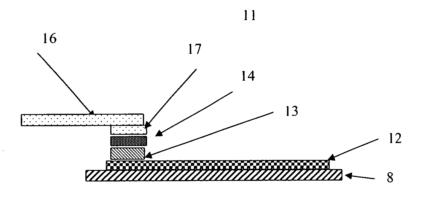
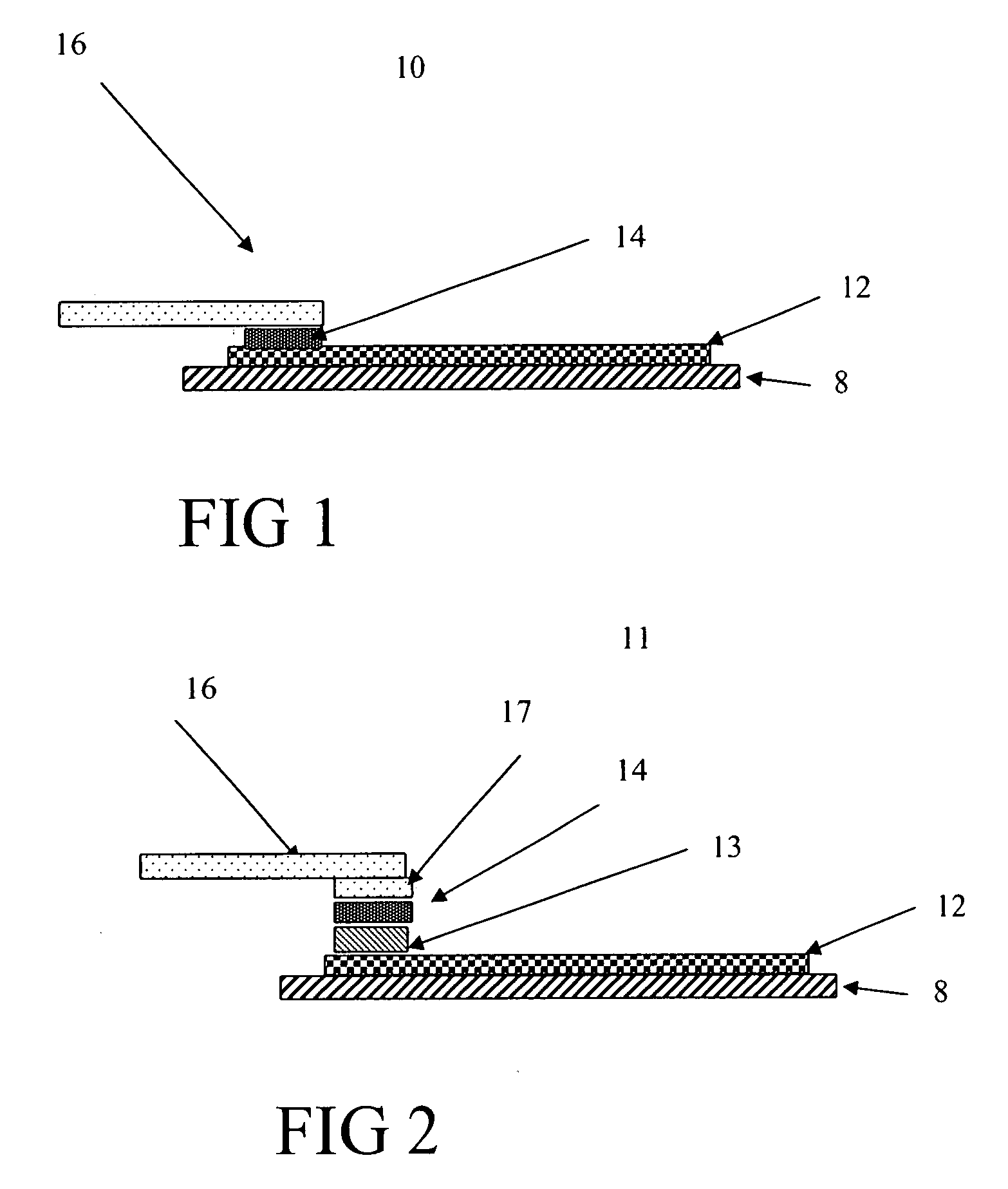
[0030]Conductive inks, dyes, and coatings currently available for producing printed or flexible electronics are formed by adding conductive materials in powder form to a polymer base with a solvent component and mixing the materials, base, and solvent to produce a uniform wet dispersion. The dispersion is used to print or apply the circuit members on the flexible non conductive polymeric film, cloth, or thread referred to as the flexible substrate. The dispersion is then cured with heat or ultraviolet light. The result is a conductive circuit formed on the flexible substrate.

[0031]In spite of the resulting circuit having a very low cost that is beneficial to the manufacturer and consumer, there are significant drawbacks such as being difficult to create a connection to another circuit component. These inks and coatings used to form these conductive traces do not have the ability to be wetted by the solder for a solder joint and have very low heat dissipation properties so that solde...


PUM

PropertyMeasurementUnit
diameteraaaaaaaaaa
lengthaaaaaaaaaa
lengthaaaaaaaaaa

Abstract

A method for producing a circuit assembly having a non-conductive substrate upon which printed conductors may be easily and selectively interconnected to another circuit assembly device, and / or apparatus.

Description

CROSS REFERENCE TO RELATED APPLICATIONS[0001]This application claims priority to U.S. Provisional Patent Application Ser. No. 60 / 851,946, filed Oct. 16, 2006, entitled “Solderable plastic components and process for soldering” and U.S. Provisional Patent Application Ser. No. 60 / 856,967, filed Nov. 6, 2006, entitled “Bondable plastic components and process for bonding,” the contents of which are both incorporated herein by reference in their entirety.FIELD OF THE INVENTION[0002]This invention generally relates to circuit assemblies such as flexible circuits and antennas and to a method for making the same and, more particularly, to a flexible type circuit assembly having at least one electrical conductor formed from a conductive ink, dye, or coating that is formulated as a wet dispersion and which further includes a portion that allows the at least one conductor to be easily, reliably, and selectively interconnected to another circuit assembly and / or to a device or apparatus by solder...

Claims


Application Information

Patent Timeline
Patent Type & Authority Applications(United States)
IPC IPC(8): H05K3/10
CPCB82Y10/00H05K1/095H05K3/245H05K3/328H05K3/361H05K3/363Y10T29/49124H05K2201/0323H05K2203/0285Y10T29/49155Y10T29/49147Y10T29/49126H05K2201/026
Inventor DOUGLAS, JOEL S.
Owner DOUGLAS JOEL S MR
Why Eureka
Try Eureka