Organic Transistor Using Self-Assembled Monolayer

a transistor and monolayer technology, applied in the field of organic transistors, can solve the problems that the formation of a self-assembled monolayer may not remarkably raise the fabrication cost, and achieve the effects of reducing the contact resistance, fabricated inexpensively, and inexpensive operation

Inactive Publication Date: 2008-04-17
HITACHI LTD
View PDF8 Cites 12 Cited by
  • Summary
  • Abstract
  • Description
  • Claims
  • Application Information

AI Technical Summary

Benefits of technology

[0021] Accordingly, it is desirable to provide a method for inexpensively reducing a contact resistance between an electrode and an organic semiconductor, which contact resistance occurs when the organic semiconductor is operated as a p-type semiconductor; and a method for inexpensively operating, as an n-type semiconductor, an organic semiconductor that is likely to work as a p-type semiconductor. In addition, it is also desirable to provide a p-cannel FET, an n-channel FET, and a complementary thin film transistor (C-TFT) which can be fabricated inexpensively. We call transistors having the same function as CMOS transistor C-TFT, independent of existence of oxides.
[0022] According to an embodiment of the present invention, a self-assembled monolayer (SAM) is formed between an electrode and an organic semiconductor. The self-assembled monolayer herein yields a sufficiently large potential difference between the two sides of the monolayer when it is adsorbed to a surface of the electrode. By the action of the potential difference, the electron level of the organic semiconductor is raised or lowered so as to control the electroconductivity as a p-type or an n-type semiconductor. Such an organic FET using an o

Problems solved by technology

The process of forming a self-assembled monolayer may not remarkably raise the fabrication cost, because it can include similar steps as in a printing process of forming another structu

Method used


Image

  • Organic Transistor Using Self-Assembled Monolayer
  • Organic Transistor Using Self-Assembled Monolayer
  • Organic Transistor Using Self-Assembled Monolayer

Examples


embodiment 1

[0028] Embodiment 1 relates to the selection of a material for self-assembled monolayer which facilitates injection of a hole from an electrode to an organic semiconductor that is likely to work as a p-type semiconductor, typified by pentacene. It also relates to a method for forming a junction structure between an electrode and an organic semiconductor using the selected self-assembled monolayer.

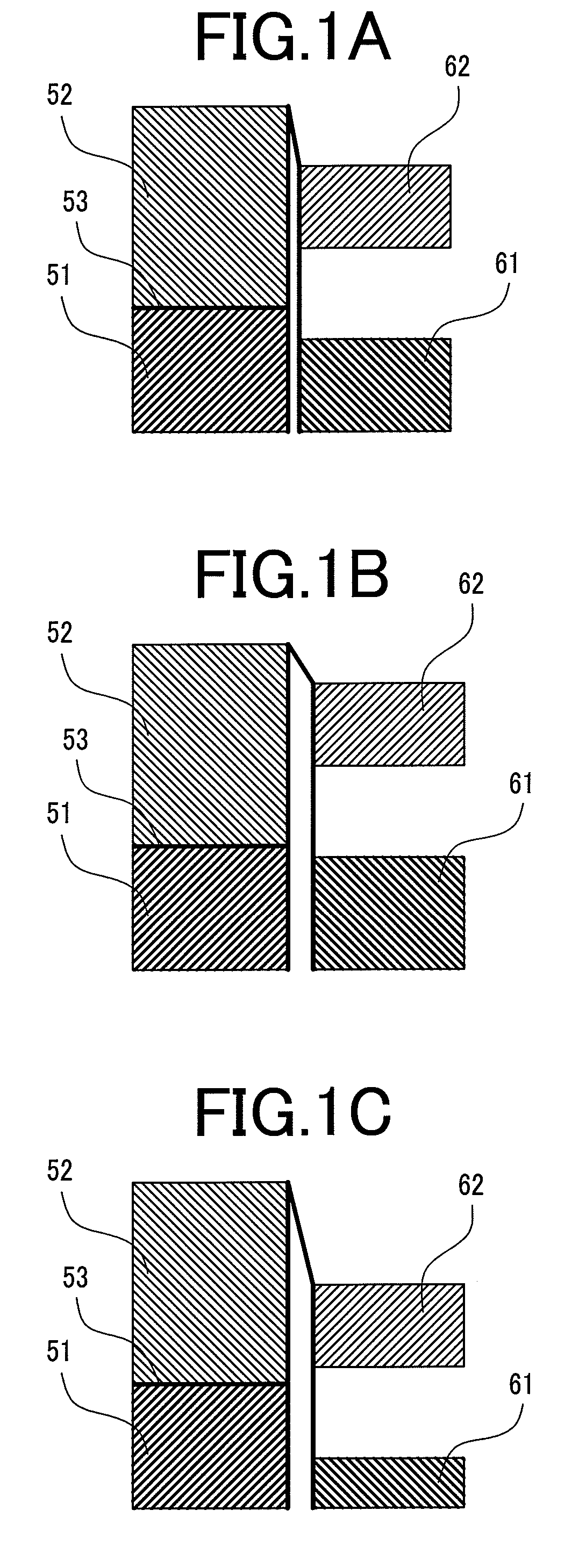
[0029] Most of organic semiconductors typified by pentacene have band gaps larger than that of silicon, in which the upper end of the valence band 61 is nearer to the Fermi level 53 of a metal constituting the electrode, such as gold, silver, or copper, than the lower end of the conduction band 62 is. Accordingly, most of such organic semiconductors are more likely to work as p-type semiconductors than to work as n-type semiconductors. Even when they are operated as p-type semiconductors, however, they invite increased contact resistance, because the upper end of the valence band of such o...

embodiment 2

[0043] Embodiment 2 relates to the selection of a material for self-assembled monolayer which enables an organic semiconductor to work as an n-type semiconductor by facilitating injection of an electron from an electrode to the organic semiconductor. The organic semiconductor employed herein is likely to work as a p-type semiconductor as a result of hole injection, typified by pentacene.

[0044] Most of organic semiconductors, such as pentacene, are more likely to work as p-type semiconductors than to work as n-type semiconductors, as described in Embodiment 1. This is because the energy difference between the Fermi level of a metal and the lower end of the conduction band of an organic semiconductor is larger than that between the Fermi level of the metal and the upper end of the valence band of the organic semiconductor. If a self-assembled monolayer causing a sufficiently large potential difference in a reverse direction to that in Embodiment 1 is available, the electron injection...

embodiment 3

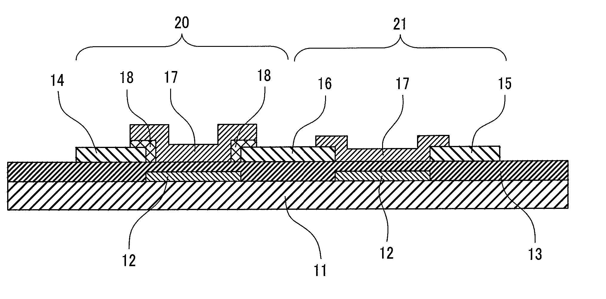
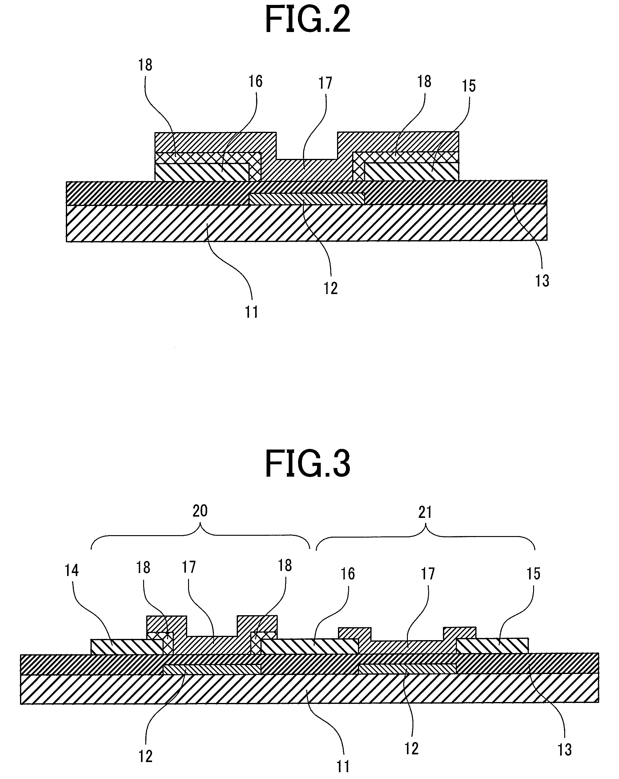
[0050] Embodiment 3 relates to a technique of constructing a C-TFT while using, as an organic semiconductor, pentacene that is likely to work as a p-type semiconductor. According to this technique, the self-assembled monolayer described in Embodiment 2 is partially arranged in specific portions between electrodes so as to allow pentacene to work as a p-type semiconductor in a specific portion and to work as an n-type semiconductor in another specific portion.

[0051]FIG. 3 is a cross sectional view schematically illustrating a structure of a C-TFT according to an embodiment (Embodiment 3) of the present invention. An organic thin-film semiconductor 17 in FIG. 3 according to Embodiment 3 is a polycrystalline pentacene thin film composed of pentacene crystal grains. The C-TFT is constituted by a source electrode 14, another source electrode 15, the organic thin-film semiconductor 17, a common drain electrode 16, and two gate electrodes 12. The C-TFT has a structure in which an n-channe...


PUM


Abstract

Disclosed are a method for inexpensively reducing the contact resistance between an electrode and an organic semiconductor upon a p-type operation of the organic semiconductor; and a method for inexpensively operating, as an n-type semiconductor, an organic semiconductor that is likely to work as a p-type semiconductor. In addition, also disclosed are a p-cannel FET, an n-channel FET, and a C-TFT which can be fabricated inexpensively. Specifically, a p-type region and an n-type region is inexpensively prepared on one substrate by arranging an organic semiconductor that is likely to work as a p-type semiconductor in a p-channel FET region and an n-channel FET region of a C-TFT; and arranging a self-assembled monolayer between an electrode and the organic semiconductor in the n-channel FET region, which self-assembled monolayer is capable of allowing the organic semiconductor to work as an n-type semiconductor.

Description

CLAIM OF PRIORITY [0001] The present application claims priority from Japanese application No. 2006-271714, filed on Oct. 3, 2006, the entire content of which is herein incorporated by reference into this application. BACKGROUND OF THE INVENTION [0002] (1) Field of the Invention [0003] The present invention relates to an organic transistor prepared through a printing process; and a method for fabricating the same. [0004] (2) Description of the Related Art [0005] Thin-film transistors (TFTs) using amorphous silicon or polycrystalline silicon as channels have been used as elements for driving picture elements in thin display devices using organic electroluminescence elements or liquid crystals. These TFTs using amorphous silicon or polycrystalline silicon are difficult to have plasticity or flexibility, and they require vacuum facilities in their fabrication process, thus generally having high fabrication costs. Accordingly, a wide variety of investigations has been made to provide TF...

Claims


Application Information

Patent Timeline
IPC IPC(8): H01L51/10H01L51/30
CPCH01L51/105H01L51/0545H10K10/84H10K10/466
Inventor SUWA, YUJIHASHIZUME, TOMIHIROANDO, MASAHIKOSHIBA, TAKEO
Owner HITACHI LTD
Why Eureka
Try Eureka