Electrostatic discharge protection devices and methods for protecting semiconductor devices against electrostatic discharge events

Active Publication Date: 2008-04-17
ADVANCED MICRO DEVICES INC
View PDF15 Cites 9 Cited by
  • Summary
  • Abstract
  • Description
  • Claims
  • Application Information

AI Technical Summary

Benefits of technology

[0006]In accordance with another exemplary embodiment of the present invention, a method for protecting an input of a semiconductor structure from an electrostatic discharge event is provided. The method comprises the steps of

Problems solved by technology

As semiconductor technology advances beyond 130 nm and 90 nm technology towards 65 nm, 45 nm, 32 nm, and even beyond, the electrostatic discharge (ESD) protection for input / output (I / O) pads and supply clamps becomes more challenging.
Present-day ESD protection circuits present a number of drawbacks, particularly when used with SOI technology.
Some ESD protection circuits suffer from high leakage current and high capacitive loading.
Other ESD protection circuits, such as those on SOI substrates, may exhibit lower leakage current and lower capacitive loading, but require thin SOI films that limit the device's ESD capability due to high self-heating, which, in turn, lowers the failure current under ESD stress.

Method used


Image

  • Electrostatic discharge protection devices and methods for protecting semiconductor devices against electrostatic discharge events
  • Electrostatic discharge protection devices and methods for protecting semiconductor devices against electrostatic discharge events
  • Electrostatic discharge protection devices and methods for protecting semiconductor devices against electrostatic discharge events

Examples


Embodiment Construction

[0016]The following detailed description of the invention is merely exemplary in nature and is not intended to limit the invention or the application and uses of the invention. Furthermore, there is no intention to be bound by any theory presented in the preceding background of the invention or the following detailed description of the invention.

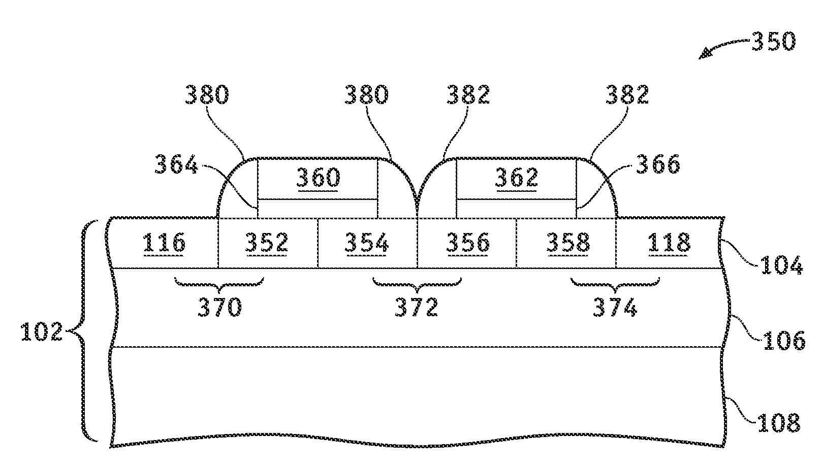
[0017]Referring to FIG. 1, an electrostatic discharge (ESD) protection device 100 in accordance with an exemplary embodiment of the present invention comprises a dual-well field effect diode (DW-FED) used for the protection of a core semiconductor circuit (not shown) against an ESD event. ESD protection device 100 comprises a silicon substrate, which may be a bulk silicon wafer (not illustrated) or, preferably, may be a thin layer of silicon 104 on an insulating layer 106 (commonly know as silicon-on-insulator or SOI) that, in turn, is supported by a carrier wafer 108. Thin silicon layer 104 typically has a thickness of about 20-100 nanomete...


PUM


Abstract

Methods and devices are provided for protecting semiconductor devices against electrostatic discharge events. An electrostatic discharge protection device comprises a silicon substrate, a P+-type anode region disposed within the silicon substrate, and an N-well device region disposed within the silicon substrate in series with the P+-type anode region. A first P-well device region is disposed within the silicon substrate in series with the first N-well device region and an N+-type cathode region is disposed within the silicon substrate. A gate electrode is disposed at least substantially overlying the first N-well and P-well device regions of the silicon substrate.

Description

FIELD OF THE INVENTION[0001]The present invention generally relates to semiconductor devices, and more particularly relates to electrostatic discharge protection devices and methods for protecting an input of a semiconductor structure from an electrostatic discharge event.BACKGROUND OF THE INVENTION[0002]As semiconductor technology advances beyond 130 nm and 90 nm technology towards 65 nm, 45 nm, 32 nm, and even beyond, the electrostatic discharge (ESD) protection for input / output (I / O) pads and supply clamps becomes more challenging. This is especially true for silicon-on-insulator (SOI) technology, which is expected to be preferable over bulk technology for the new process nodes. An ESD event refers to a phenomenon of electrical discharge of a current (positive or negative) for a short duration during which a large amount of current is provided to a semiconductor structure.[0003]Present-day ESD protection circuits present a number of drawbacks, particularly when used with SOI tech...

Claims


Application Information

Patent Timeline
IPC IPC(8): H01L23/62H01L21/8238
CPCH01L29/7436H01L27/0262H01L27/0259H01L27/02
Inventor SALMAN, AKRAMBEEBE, STEPHEN
Owner ADVANCED MICRO DEVICES INC
Why Eureka
Try Eureka