Semiconductor device having contact barrier and method of manufacturing the same

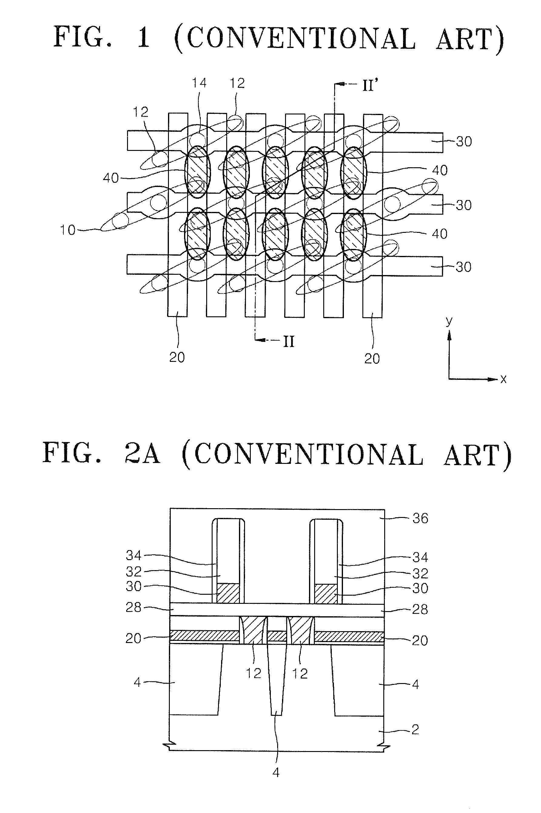
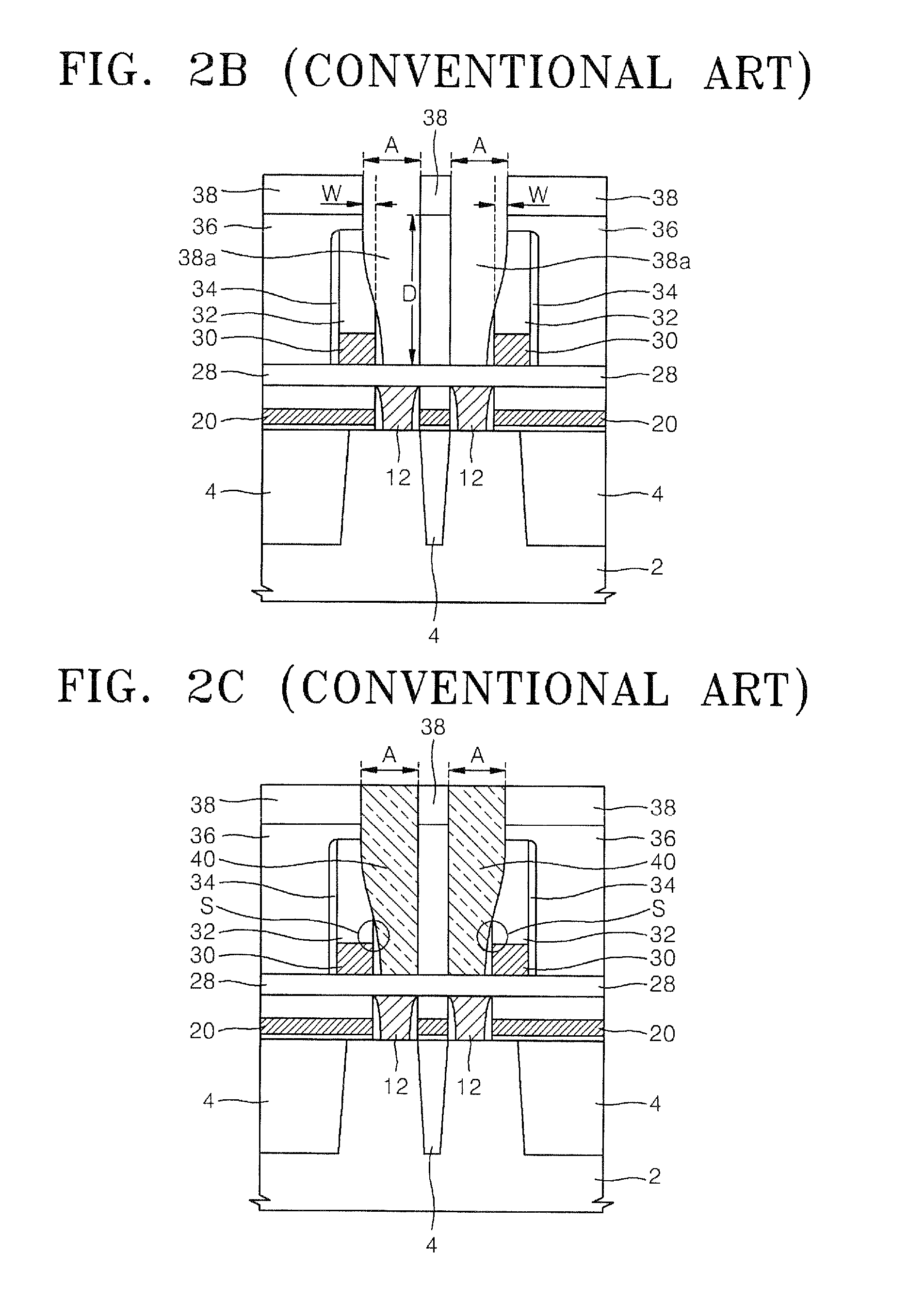
a technology of semiconductor devices and contact barriers, which is applied in the direction of semiconductor devices, semiconductor/solid-state device details, electrical apparatus, etc., can solve the problems of inconvenient manufacturing of the same, the bottom area of the buried contact b>40/b> becomes undetectable narrow, and the difficulty of fine contact holes for implementing highly integrated devices using conventional photolithography processes

Active Publication Date: 2008-04-17
SAMSUNG ELECTRONICS CO LTD
View PDF12 Cites 6 Cited by
  • Summary
  • Abstract
  • Description
  • Claims
  • Application Information

AI Technical Summary

Benefits of technology

[0012] Exemplary embodiments of the present invention can be characterized as providing a highly integrated semiconductor device having various layouts and having a structure in which short circuits between a contact with a large aspect ratio and a conductive layer around the contact and failures generated due to the short circuits can be prevent

Problems solved by technology

As a result, it is difficult to form fine contact holes for implementing highly integrated devices using conventional ph

Method used


Image

  • Semiconductor device having contact barrier and method of manufacturing the same
  • Semiconductor device having contact barrier and method of manufacturing the same
  • Semiconductor device having contact barrier and method of manufacturing the same

Examples


Embodiment Construction

[0028] Embodiments of the present invention will now be described more fully hereinafter with reference to the accompanying drawings, in which preferred embodiments of the invention are shown. These embodiments may, however, be realized in many different forms and should not be construed as being limited to the embodiments set forth herein. Rather, these embodiments are provided so that this disclosure will be thorough and complete, and will fully convey the scope of the invention to those skilled in the art. In the drawings, the thickness of layers, films and regions are exaggerated for clarity. Like numbers refer to like elements throughout the specification.

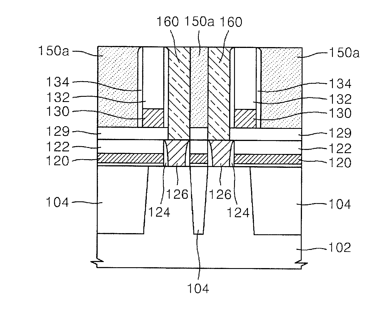
[0029]FIG. 3 is a schematic view of a semiconductor device according to one embodiment. It will be appreciated that the semiconductor device schematically illustrated in FIG. 3 may be applied to a memory cell having, for example, a unit cell size of 6F2. FIG. 4 is a cross-sectional view taken along line IV-IV′ shown in FIG. 3...


PUM


Abstract

A semiconductor device having a contact barrier for insulating contacts with a large aspect ratio and having a fine pitch between adjacent conductive lines and a method of manufacturing the same are provided. The semiconductor device includes a buried contact formed in a region between two adjacent first conductive lines and two adjacent second conductive lines. Insulating lines define a width of the buried contact. To form the contact barrier, an interlayer dielectric layer formed on the second conductive lines is patterned to form a space and an insulating line having an etching ratio different from the interlayer dielectric layer is formed in the space. The interlayer dielectric layer is selectively wet etched relative to an insulating layer covering the second conductive line and the first insulating line to form buried contact hole. The buried contact hole is filled with conductive material to form a buried contact.

Description

CROSS-REFERENCE TO RELATED PATENT APPLICATION [0001] This application is a continuation-in-part of U.S. patent application Ser. No. 11 / 751,515, filed on May 21, 2007, now pending, which is a divisional of U.S. patent application Ser. No. 11 / 143,197, filed on Jun. 1, 2005, now pending, which is a divisional of U.S. patent application Ser. No. 10 / 697,722, filed on Oct. 29, 2003, now U.S. Pat. No. 6,916,738, issued on Jul. 12, 2005, which claims priority from Korean Patent Application No. 2003-11310, filed on Feb. 24, 2003, and also claims the benefit of foreign priority to Korean Patent Application No. 2007-46193, filed on May 11, 2007, the disclosures of which are incorporated herein in their entirety by reference.BACKGROUND [0002] 1. Field of Invention [0003] Embodiments of the present invention relate generally to semiconductor devices having contact barriers and methods of manufacturing the same. More particularly, embodiments of the present invention relate to a semiconductor dev...

Claims


Application Information

Patent Timeline
IPC IPC(8): H01L23/48H01L21/4763
CPCH01L21/76802H01L27/0207H01L27/10885H01L27/10855H01L27/10808Y10S257/905H10B12/31H10B12/0335H10B12/482
Inventor HONG, HYEONG-SUNLEE, JAE-GOOKIM, DONG-HYUNKWON, SUNG-UNPARK, SANG-JOONKANG, NAM-JUNG
Owner SAMSUNG ELECTRONICS CO LTD
Why Eureka
Try Eureka