Organic electroluminescence element and manufacturing method thereof

Inactive Publication Date: 2005-02-15
IDEMITSU KOSAN CO LTD
View PDF11 Cites 17 Cited by
  • Summary
  • Abstract
  • Description
  • Claims
  • Application Information

AI Technical Summary

Benefits of technology

[0067]By configuring in this way, the second electrode may be mechanically and chemically protected, and furthermore

Problems solved by technology

Consequently, with regard to the light transmittance of the electrode, there are problems in that the electrode material is limited to transparent material, such as indium tin oxide (ITO) or the blue light is dif

Method used


Image

  • Organic electroluminescence element and manufacturing method thereof
  • Organic electroluminescence element and manufacturing method thereof
  • Organic electroluminescence element and manufacturing method thereof

Examples


Example

Example 1

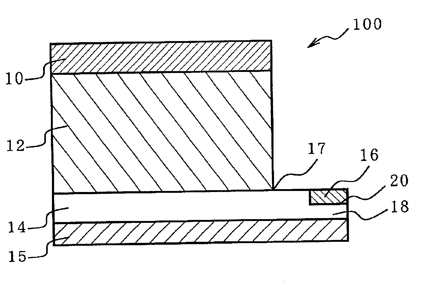
[0214](1) Fabrication of Organic EL Element

[0215](i) Formation of the Cathode (Second Electrode)

[0216]A transparent glass substrate having a dimension of 1.1 mm(thickness)×200 mm (length)×200 mm (width) was ultrasonically cleaned and after drying in the N2 (nitrogen gas) environment, the glass substrate was cleaned by the use of UV (ultraviolet ray) and ozone further for 10 minutes. Then, on the cleaned glass substrate, a thin film (100 nm thick) comprising Al / Si alloy (Si concentration: 1 at. %) was formed by the use of the sputtering apparatus (available from ULVAC JAPAN, Ltd.). This Al / Si alloy thin film was patterned in lattices (line width: 20 μm; lattice pitch: 320 μm) by the use of photolithography as shown in FIG. 11(a). The construction of the configuration in which the cathode (second electrode) was electrically connected at the edge section of the semiconductor layer was intended.

[0217](ii) Formation of the Semiconductor Layer

[0218]The glass substrate on which th...

Example

Example 2

[0230](1) Formation of Organic EL Element

[0231](i) Formation of the Anode (Second Electrode)

[0232]Same as Example 1, the Al / Si alloy thin film patterned in the form of lattices (line width: 20 μm; lattice pitch: 320 μm) was formed and designated it as the anode (second electrode).

[0233](ii) Formation of the Semiconductor Layer

[0234]The glass substrate with the anode formed was cleaned with argon plasma, and then, on this glass substrate, using the vacuum deposition apparatus (available from ULVAC JAPAN, Ltd.), CdS and Cu are simultaneously deposited in 30 nm film thickness to form the p-type semiconductor layer. The deposition was carried out at the vacuum of 1×10⁻⁶ Torr (1.33×10⁻⁴ Pa) and at the substrate temperature of 160° C., and Cu deposition was carried out so that the specific resistance of the semiconductor layer satisfied 2×10 Ω≠cm. The charge concentration of the semiconductor layer was measured by the four-terminal method and it was confirmed that the charge conc...

Example

Example 3

[0242](1) Fabrication of Organic EL Element

[0243]In Example 3, effects of the organic semiconductor layer were investigated. That is, in place of the semiconductor layer comprising a combination of CdS and Cu in Example 2, a 70-nm-film thickness semiconductor layer comprising PEDOT (3,4-polyethylene dioxythiophene, available from Bayer), which is polymer indicating semiconductance, was spin-coated in the condition of the aqueous solution, and then, was vacuum-dried to form an organic EL element, with others all same as Example 2.

[0244](2) Assessment of the Organic EL Element

[0245]When DC7V voltage was applied across the cathode (first electrode) and the anode (second electrode), the 5.2 mA / cm2 current flew and green light emission which emission luminance was 180 cd / m2 was obtained via the semiconductor layer. Then, when the organic EL element was driven at constant current with the initial emission luminance set to 100 cd / m2, the 790-hour half-life was obtained. The result...


PUM


Abstract

The present invention relates to an organic electroluminescence element and the manufacturing method thereof comprising an anode, semiconductor layer, organic light-emitting medium, and a cathode, an organic light-emitting medium is located between the first electrode and the semiconductor layer comprising the non-monocrystal material and the second electrode is electrically connected to the edge section of the semiconductor layer when either one of the anode or cathode is designated to the first electrode and the other electrode to the second electrode.
Because the first electrode and the second electrode are configured in such a manner not to be opposite to each other in this way, various electrode materials are able to be used and the light-emitting area is able to be increased, and therefore, the organic EL element with the luminous energy taken out to the outside and a manufacturing method that can efficiently obtain such organic EL element are able to be provided.

Description

CROSS REFERENCE TO RELATED APPLICATION[0003]This is a continuation application of PCT International Application of PCT / JP00 / 02796 filed on Apr. 27, 2000.BACKGROUND OF THE INVENTION[0004]1. Field of Invention[0005]The present invention relates to an organic electroluminescence element (hereinafter sometimes called the “organic EL element” or “EL element”) and the manufacturing method thereof.[0006]Particularly, the present invention relates to an organic EL element which has a large light-emitting area suited for noncommercial and industrial-use display devices (liquid displays and the like) and which can be used for various electrode materials and to the manufacturing method that can obtain such organic EL elements efficiently.[0007]2. Description of Related Art[0008]One example of the conventional organic EL element is disclosed in, for example, JP-A-3-262170. Referring now to FIG. 13, the configuration is explained. An organic layer 202 is interposed between a first electrode 201 ...

Claims


Application Information

Patent Timeline
IPC IPC(8): H01L51/52H01L51/50H01L27/32
CPCH01L51/5203H01L51/5221H01L51/5206H01L27/32H01L2251/5361H10K59/00H10K50/805H10K50/81H10K50/814H10K50/822H10K50/824H05B33/26
Inventor HOSOKAWA, CHISHIOKAWAMURA, HISAYUKINAKAMURA, HIROAKI
Owner IDEMITSU KOSAN CO LTD
Why Eureka
Try Eureka