This helps you quickly interpret patents by identifying the three key elements:
Problems solved by technology
Method used
Benefits of technology
Benefits of technology
[0013]The first aspect of the present invention can form a flat solid polyelectrolyte layer (short-circuit prevention coating film) having a uniform thickness on the surface of the active material layer. Operations and advantageous effects of the first aspect of the present invention will be explained in detail in the following.
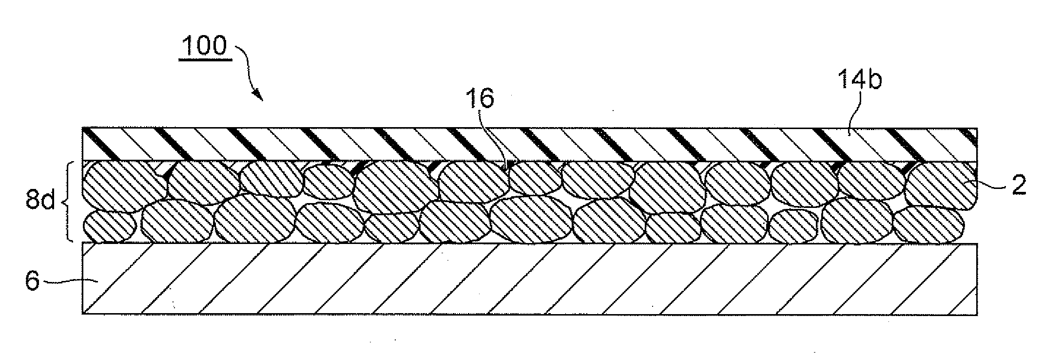
[0014]After applying the second solvent to the surface of a coating film which is a precursor of an active material layer, the first aspect of the present invention applies a solid polyelectrolyte layer coating material (SPE layer coating material) to the surface of the coating film, thereby forming a precursor (SPE layer precursor) of the solid polyelectrolyte layer (SPE layer). Removing the first, second, and third solvents yields an electrode comprising a current collector, an active material layer formed on the current collector, and an SPE layer formed on the active material layer.
[0015]Though the coating film surface tends to incur irregularities in conformity to forms of active material particles contained in the coating film, the first aspect of the present invention eliminates the irregularities on the coating film surface by covering the coating film with the second solvent. Applying the SPE layer coating material onto thus flattened coating film surface can form a flat SPE layer precursor having a uniform thickness. Hence, the SPE layer precursor can be inhibited from partly retracting into recesses of the coating film surface or projecting at protrusions of the coating film surface. Since the second solvent is a poor solvent for the SPE layer binder, the SPE layer precursor formed on the coating film surface covered with the second solvent is harder to be dissolved by the second solvent and can keep a flat form with a uniform thickness. That is, the SPE layer binder binding pieces of the SPE to each other in the SPE layer precursor is hard to be dissolved by the second solvent, whereby the SPE layer precursor keeps a flat form with a uniform thickness. Removing the solvent from within the SPE layer precursor thus kept in a flat form with a uniform thickness can yield a flat SPE layer with a uniform thickness. An electrochemical device using an electrode equipped with such a flat SPE layer with a uniform thickness can prevent short circuits from occurring between electrodes.
[0016]Since a wet SPE layer coating material is applied to the coating film surface kept in a wet (humid) state by the second solvent, the first aspect of the present invention improves the adhesion between the resulting active material layer and the SPE layer as compared with the case where the SPE layer coating material is applied to a dry (dried) coating film. A part of the SPE layer binder contained in the SPE layer coating material comes into contact with the second solvent (the poor solvent for the SPE layer binder) on the coating film surface, so as to be deposited between the SPE layer precursor and the coating film. Hence, on the SPE layer side of the active material layer in the resulting electrode, the SPE layer binder bonds the active material particles together and to the SPE layer, thereby improving the adhesion between the active material layer and the SPE layer. Thus improving the adhesion between the active material layer and the SPE layer can prevent the SPE layer from peeling and shifting, thereby avoiding short circuits in electrochemical devices.
[0017]In the first aspect of the present invention, the first solvent may be removed from the coating film before the second step. Removing the good solvent from the coating film allows the active material layer binder deposited within the coating film to bind pieces of the active material together. The advantageous effects of the present invention can also be attained when the second solvent is thus applied to the coating film after drying the coating film.
[0018]Preferably, in the first aspect of the present invention, the coating film coated with the second solvent is pressed before the third step. Pressing the coating film coated with the second solvent reduces the irregularities on the coating film surface, thereby making it easier to form a flat SPE layer precursor with a uniform thickness on the coating film surface.
Problems solved by technology
The coating material applied to such a surface of the active material layer covers the same in conformity to the irregularities, the resulting short-circuit prevention coating film tends to incur irregularities instead of becoming flat.
Such a nonflat short-circuit prevention coating film tends to peel off from the positive or negative electrode, shift from a predetermined position, or break because of a vibration or a shutdown at a high temperature, thereby causing a short circuit.
Method used
Image
Click on the blue label to locate the original text in one second.
Reading with bidirectional positioning of images and text.
[0047]The electrode manufacturing method in accordance with the first embodiment comprises a step (first step: S1) of applying an active material layer coating material containing active material particles, an active material layer binder, and a first solvent to a current collector so as to form a coating film made of the active material layer coating material; a step (first solvent removing step: S2) of removing the first solvent from the coating film; a step (second step: S3) of applying a second solvent to the coating film having removed the first solvent; a step (third step: S4) of applying an SPE layer coating material containing a solid polyelectrolyte (SPE), an SPE layer binder, and a third solvent to the coating film coated with the second solvent; and a step (solvent removing step: S5) of removing the second and third solvents from the coating film and the SPE layer precursor.
[0048]The first solvent is a good solvent for the active material lay...
second embodiment
[0095]The electrode manufacturing method in accordance with the second embodiment of the present invention will now be explained. Here, while omitting matters common in the first and second embodiments, only their differences will be explained.
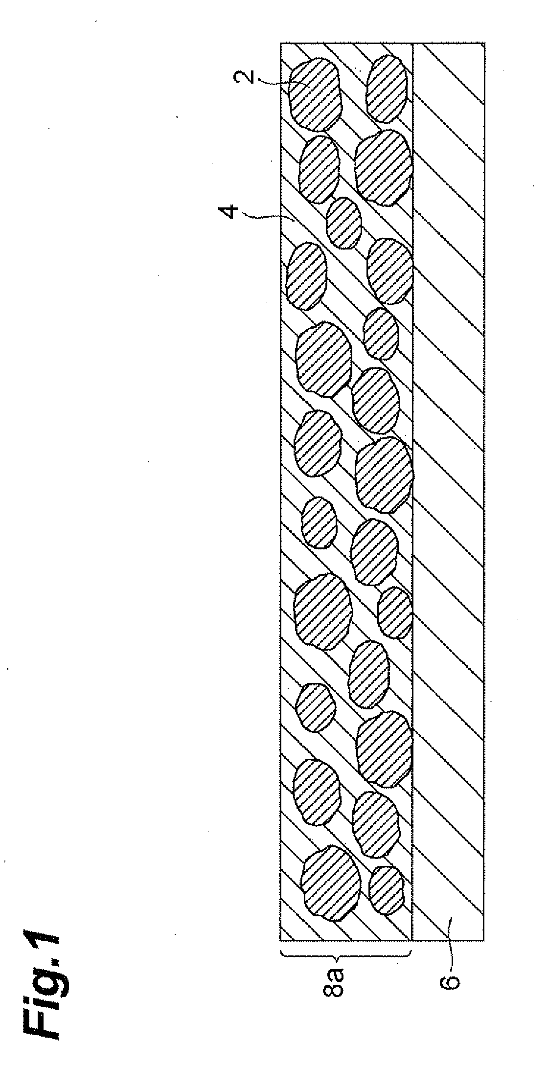
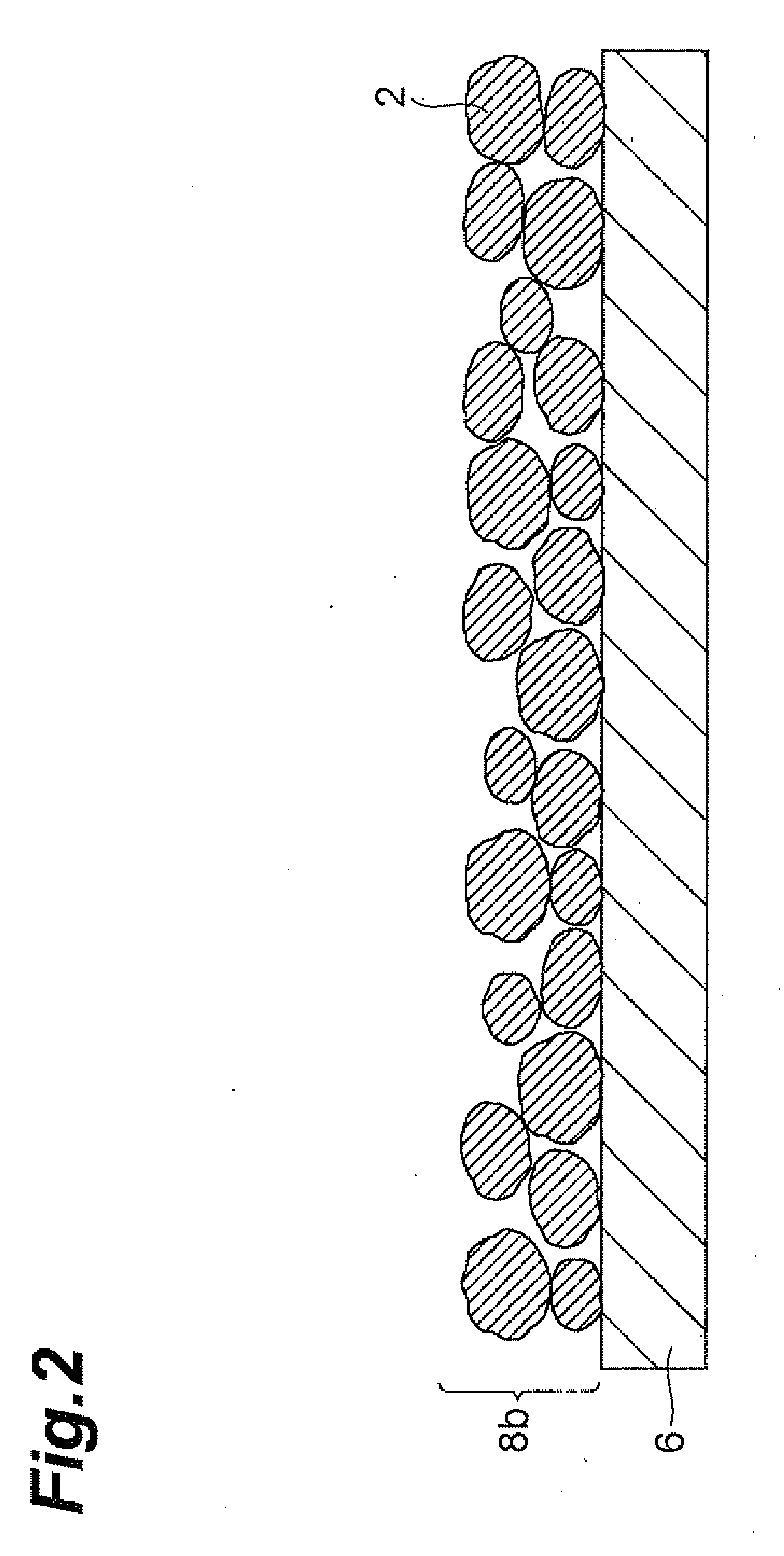
[0096]Unlike the first embodiment, the second embodiment does not use the second solvent. The first solvent 4 is a good solvent for the active material layer binder and a poor solvent for the SPE layer binder, while the third solvent is a good solvent for the SPE layer binder.
[0097]As illustrated in FIG. 6, the electrode manufacturing method in accordance with the second embodiment applies an active material layer coating material containing active material particles 2, an active material layer binder, and the first solvent 4 to a current collector 6, so as to form a coating film 8a (active material layer precursor) made of the active material layer coating material.
[0098]Next, an SPE layer coating material containing an SPE, an SPE layer bind...
[0109]Active material particles made of graphite (product name: OMAC, manufactured by Osaka Gas Chemicals Co. Ltd.), PVDF (homopolymer; product name: 761, manufactured by Atofina) as an active material layer binder, and carbon black (product name: DAB, manufactured by Denki Kagaku Kogyo K.K.) as a conductive auxiliary were dispersed into NMP, which was a good solvent (first solvent) for the active material layer, so as to prepare a negative electrode coating material.
[0111]A VDF copolymer (copolymer of vinyl fluoride and propylene hexafluoride; product name: 2801, manufactured by Atofina), which was a solid polyelectrolyte, and a VDF copolymer (copolymer of vinyl fluoride and propylene hexafluoride; product name: 2801, manufactured by Atofina), which was an SPE layer binder, were dispersed into acetone, which was a good solvent (third solvent) for the SPE layer binder, so as to prepare an SPE l...
PUM
Abstract
An electrode manufacturing method which can form a flat short-circuit prevention coating film (solidpolyelectrolyte layer) having a uniform thickness and prevent short circuits from occurring in an electrochemical device is provided. The electrode manufacturing method comprises a first step of applying an active material layer coating material containing an active material particle, an active material layer binder, and a first solvent to a current collector so as to form a coating film made of the active material layer coating material; a second step of applying a second solvent to the coating film; and a third step of applying a solidpolyelectrolyte layer coating material containing a solidpolyelectrolyte, a solid polyelectrolyte layer binder, and a third solvent to the coating film coated with the second solvent. The first solvent is a good solvent for the active material layer binder, the second solvent is a poor solvent for the solid polyelectrolyte layer binder, and the third solvent is a good solvent for the solid polyelectrolyte layer binder.
Description
BACKGROUND OF THE INVENTION[0001]1. Field of the Invention[0002]The present invention relates to an electrode manufacturing method and an electrode.[0003]2. Related Background Art[0004]Electrochemical devices such as secondary batteries including lithium-ion secondary batteries and electrochemical capacitors including electric double layer capacitors are easy to reduce their size and weight, and thus are promising as power supplies or backup power supplies for portable devices (small-size electronic devices) and auxiliary power supplies for electric cars and hybrid cars, for example, whereby various studies have been under way in order to improve their safety.[0005]In the electrochemical devices disclosed in Japanese Patent Application Laid-Open Nos. 10-106546, 11-185731, 11-288741, 2001-325951, and 2007-005323, the surface of an active material layer of a positive or negative electrode is covered with a coating film (hereinafter referred to as “short-circuit prevention coating film...
Claims
Application Information
Patent Timeline
Application Date:The date an application was filed.
Publication Date:The date a patent or application was officially published.
First Publication Date:The earliest publication date of a patent with the same application number.
Issue Date:Publication date of the patent grant document.
PCT Entry Date:The Entry date of PCT National Phase.
Estimated Expiry Date:The statutory expiry date of a patent right according to the Patent Law, and it is the longest term of protection that the patent right can achieve without the termination of the patent right due to other reasons(Term extension factor has been taken into account ).
Invalid Date:Actual expiry date is based on effective date or publication date of legal transaction data of invalid patent.

