Optical thin film, semiconductor light emitting device having the same and methods of fabricating the same

a technology of optical thin film and semiconductor light emitting device, which is applied in the direction of optics, optical elements, instruments, etc., to achieve the effects of reducing optical output loss, maximizing or increasing light transmittance efficiency, and improving structur

Active Publication Date: 2008-04-17
RENESSELAER POLYTECHNIC INST +1
View PDF36 Cites 55 Cited by
  • Summary
  • Abstract
  • Description
  • Claims
  • Application Information

AI Technical Summary

Benefits of technology

[0017]According to example embodiments, the optical thin film having an improved structure, in which, optical or Fresnel reflection (due to a difference in the refractive index between a semiconductor material and the ambient material (for example, air and/or an encapsulation material), ...

Problems solved by technology

However, in conventional LEDs having such a structure, there may be limitations when addressing current technical objectives, for example, a ...

Method used


Image

  • Optical thin film, semiconductor light emitting device having the same and methods of fabricating the same
  • Optical thin film, semiconductor light emitting device having the same and methods of fabricating the same
  • Optical thin film, semiconductor light emitting device having the same and methods of fabricating the same

Examples


Embodiment Construction

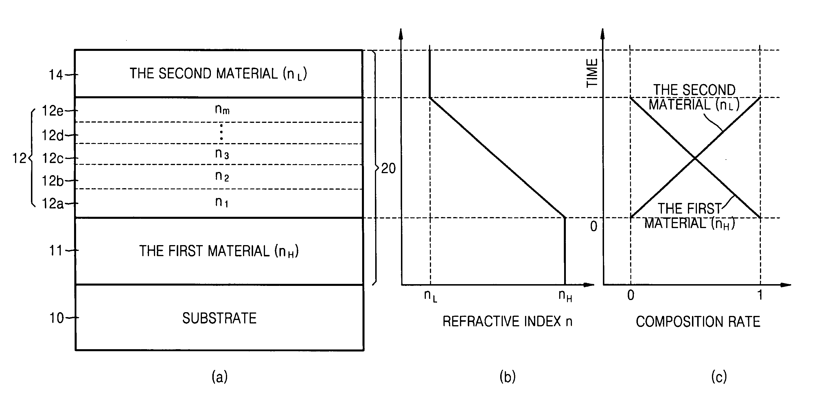
[0032]Example embodiments will now be described more fully with reference to the accompanying drawings, in which example embodiments are shown. In example embodiments, the first layer, the second layer, and the graded-index layer interposed or inserted between the first layer and the second layer may be deposited by co-deposition method. In other example embodiments, the first layer, the second layer, and the graded-index layer interposed or inserted between the first layer and the second layer may be deposited by oblique deposition method. In the drawings, the thicknesses of layers and regions are exaggerated for clarity.

[0033]It will be understood that when an element or layer is referred to as being “on,”“connected to” or “coupled to” another element or layer, it can be directly on, connected or coupled to the other element or layer or intervening elements or layers may be present. In contrast, when an element is referred to as being “directly on,”“directly connected to” or “dire...


PUM


Abstract

Provided are a highly transmissive optical thin film having an improved structure, in which, optical reflection (due to a difference in the refractive index between a semiconductor material and the air, when light is extracted from a semiconductor light emitting device into the air) may be suppressed, an optical output loss may be reduced and light transmittance efficiency may be maximized or increased, a semiconductor light emitting device having the same, and methods of fabricating the same. The optical thin film may include a first material layer having a first refractive index, a second material layer formed on the first material layer and having a second refractive index that is smaller than the first refractive index, and a graded-refractive index layer interposed or inserted between the first material layer and the second material layer and having a multi-layer structure in which refractive index distribution gradually decreases in the range between the first refractive index and the second refractive index as the refractive index distribution progresses from the first material layer toward the second material layer.

Description

PRIORITY STATEMENT[0001]This application claims priority under 35 USC § 119 to U.S. Provisional Application No. 60 / 850,657, filed on Oct. 11, 2006, in the United States Patent and Trademark Office (USPTO), the entire contents of which are herein incorporated by reference.BACKGROUND[0002]1. Field[0003]Example embodiments relate to a semiconductor light emitting device. Other example embodiments relate to a highly transmissive optical thin film having an improved structure, in which, optical reflection (due to a difference in the refractive index between a semiconductor material and the air, when light is extracted from a semiconductor light emitting device into the surrounding medium (e.g., an encapsulation material)) may be suppressed, an optical output loss may be reduced and light transmittance efficiency may be maximized or increased, and a semiconductor light emitting device having the same. Other example embodiments relate to methods of fabricating the same.[0004]2. Description...

Claims


Application Information

Patent Timeline
IPC IPC(8): G02B1/10
CPCG02B1/113
Inventor CHO, JAE-HEEMONT, FRANK WILHELMSONE, CHEOL-SOOKIM, JONG-KYUSONG, JUNE-OSCHUBERT, E. FRED
Owner RENESSELAER POLYTECHNIC INST
Why Eureka
Try Eureka