Crossbar-memory systems and methods for writing to and reading from crossbar memory junctions of crossbar-memory systems

a technology of crossbar memory and crossbar memory, applied in the field methods for writing to and reading from crossbar memory junctions of crossbar memory system, can solve the problems of irreversible destruction of crossbar-memory junctions to which the greater voltage is applied, and many new problems

Inactive Publication Date: 2008-04-17
HEWLETT-PACKARD ENTERPRISE DEV LP
View PDF8 Cites 129 Cited by
  • Summary
  • Abstract
  • Description
  • Claims
  • Application Information

AI Technical Summary

Problems solved by technology

However, the design and manufacture of nanoscale electronic devices present many new problems that need to be addressed prior to large-scale commercial production of nanoscale electronic devices and incorporation of nanoscale electronic devices into microscale and larger-scale systems, devices, and products.
However, application of voltages greater in magnitude than the voltages used to reversibly configure crossbar-memory junctions can irreversibly destroy the crossbar-memory junctions to which the greater voltages are applied.

Method used


Image

  • Crossbar-memory systems and methods for writing to and reading from crossbar memory junctions of crossbar-memory systems
  • Crossbar-memory systems and methods for writing to and reading from crossbar memory junctions of crossbar-memory systems
  • Crossbar-memory systems and methods for writing to and reading from crossbar memory junctions of crossbar-memory systems

Examples


first embodiment

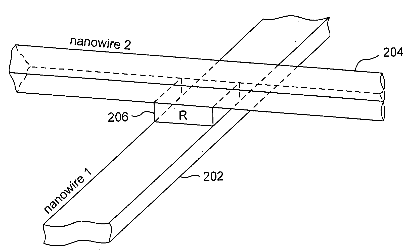
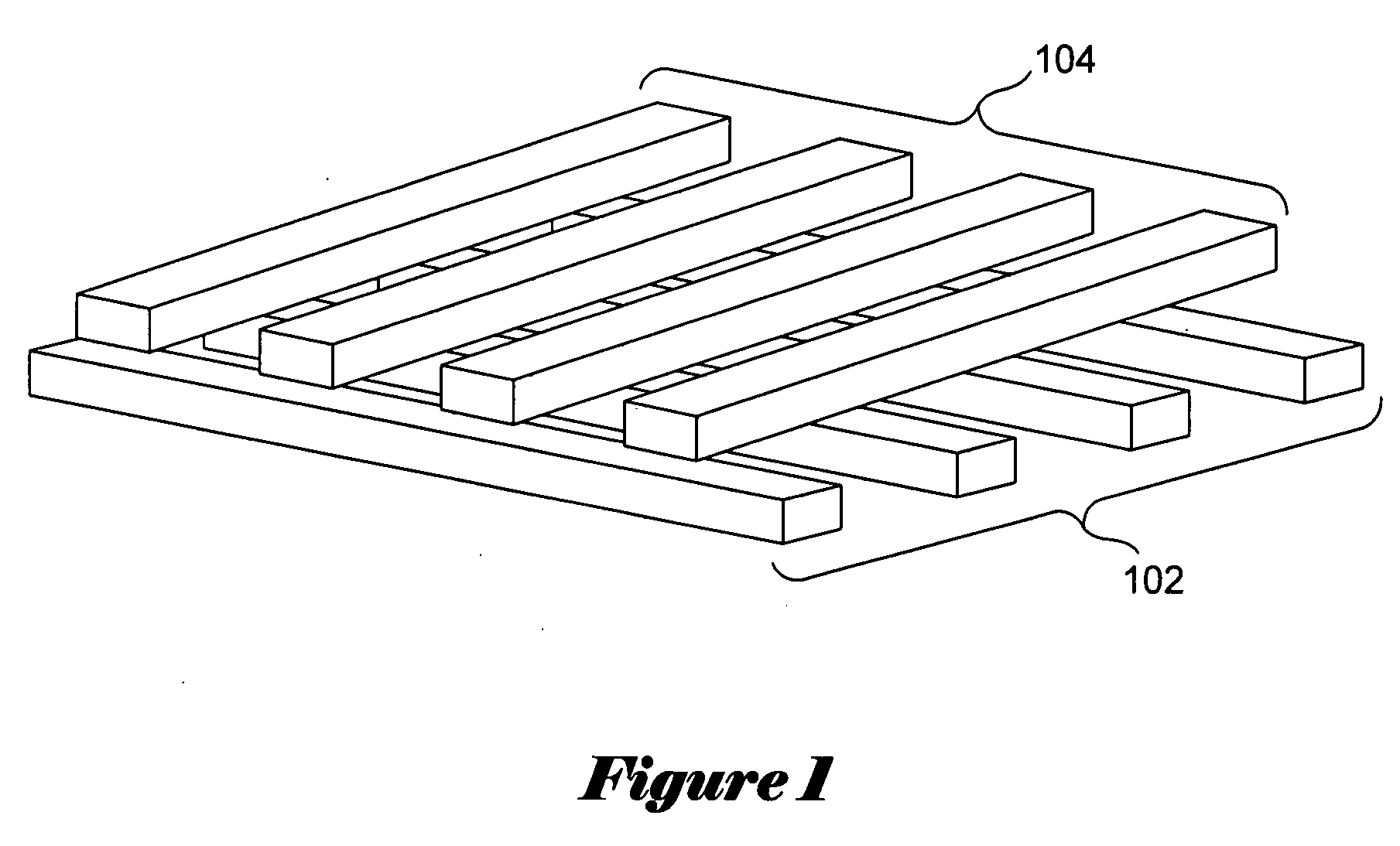
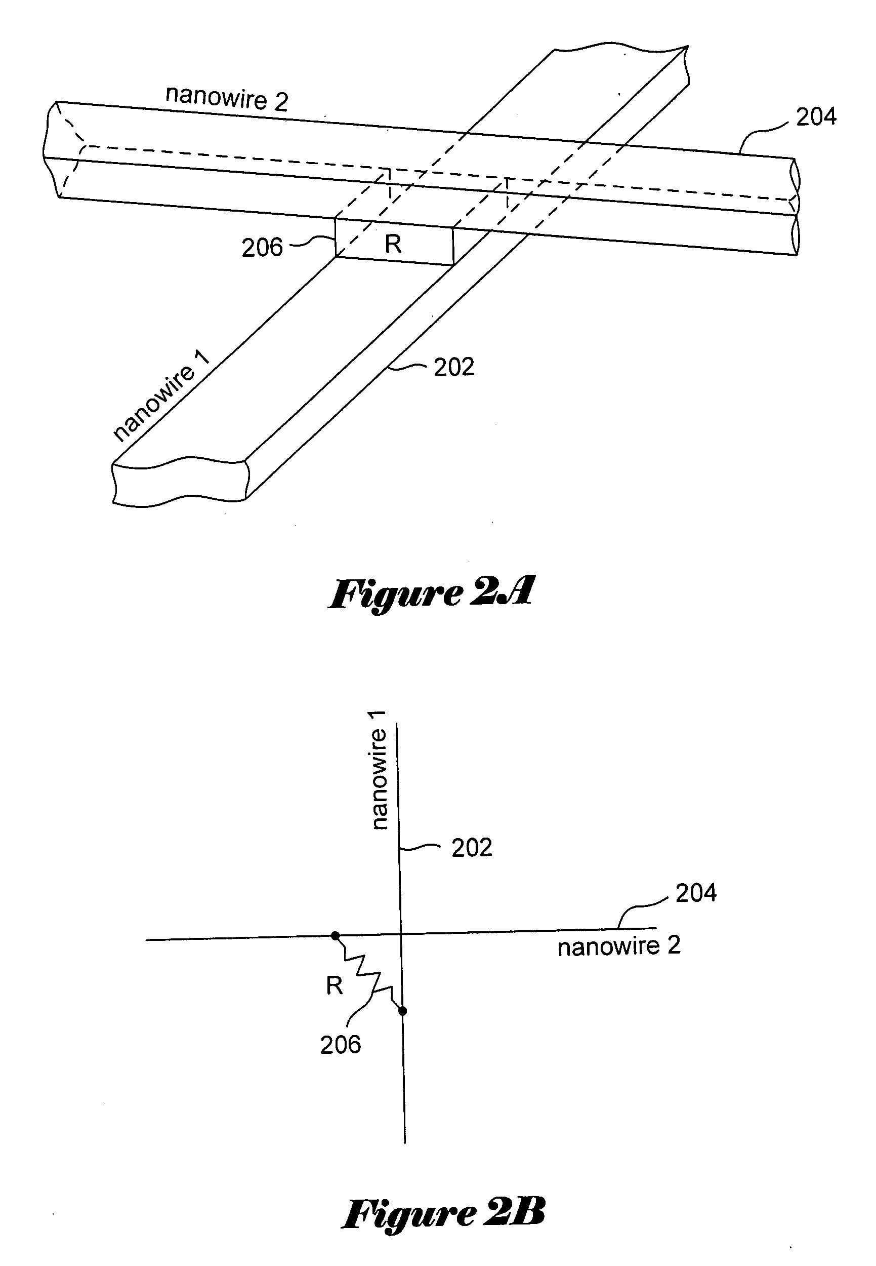
[0082]FIG. 13 illustrates an example crossbar-memory system 1300 configured to store and retrieve information that represents the present invention. The crossbar-memory system 1300 comprises a 9×9 nanowire-crossbar array 1302, a first combined microscale / nanoscale encoder-demultiplexer 1304, and a second combined microscale / nanoscale encoder-demultiplexer 1306. A nonlinear-tunneling-hysteretic resistor (not shown) is located at each crossbar junction of the crossbar array 1302. The crossbar array 1302 includes an 8×8 crossbar-memory array 1308. A column nanowire 1310 and a row nanowire 1312 of the crossbar array 1302 are dedicated to serve as wires in a switched-based row multiplexer (“mux”) 1314 and a column mux 1316, respectively, which can both be used to isolate selected crossbar memory junctions of the crossbar-memory array 1308. For example, the row mux 1314 and column mux 1316 can be used isolate a selected crossbar memory junction 1318 so that an unknown memory state of the ...

second embodiment

[0083]In alternate embodiments of the present invention, the column mux and row mux may be separated spatially from the crossbar array and can be made with wires having cross-sectional dimensions ranging from the nanoscale to microscale in order to lower the impedance. In addition, the a and k parameters of the nonlinear-tunneling-hysteretic resistors connecting the overlapping row and column nanowires of the crossbar-memory array can be different from the a and k parameters of the nonlinear-tunneling-hysteretic resistors connecting the row and column wires in the row and column muxes. FIG. 14 illustrates an example configuration of a crossbar-memory system 1400 that is structurally similar to the crossbar-memory system 1300 shown in FIG. 13 and represents the present invention. In the interest of brevity, structurally identical components in both of the crossbar-memory systems 1300 and 1400 have been provided with the same reference numerals and an explanation of their structure an...


PUM


Abstract

Various embodiments of the present invention are directed to crossbar-memory systems to methods for writing information to and reading information stored in such systems. In one embodiment of the present invention, a crossbar-memory system comprises a first layer of microscale signal lines, a second layer of microscale signal lines, a first layer of nanowires configured so that each first layer nanowire overlaps each first layer microscale signal line, and a second layer of nanowires configured so that each second layer nanowire overlaps each second layer microscale signal line and overlaps each first layer nanowire. The crossbar-memory system includes nonlinear-tunneling resistors configured to selectively connect first layer nanowires to first layer microscale signal lines and to selectively connect second layer nanowires to second layer microscale signal lines. The crossbar-memory system also includes nonlinear tunneling-hysteretic resistors configured to connect each first layer nanowire to each second layer nanowire at each crossbar intersection.

Description

TECHNICAL FIELD[0001]The present invention is related to nanoscale and combined microscale / nanoscale electronics and, in particular, to crossbar-memory systems configured so that information can be written to, and read from, crossbar memory junctions of the crossbar-memory systems.BACKGROUND OF THE INVENTION[0002]Significant research and development efforts are currently directed towards designing and manufacturing nanoscale electronic devices, including nanoscale memories. Nanoscale electronics promise a number of advantages over microscale, photolithography-based electronics, including significantly reduced features sizes and the potential for self-assembly and for other relatively inexpensive, non-photolithography-based fabrication methods. However, the design and manufacture of nanoscale electronic devices present many new problems that need to be addressed prior to large-scale commercial production of nanoscale electronic devices and incorporation of nanoscale electronic device...

Claims


Application Information

Patent Timeline
Patent Type & Authority Applications(United States)
IPC IPC(8): G11C11/00
CPCB82Y10/00G06F11/1008G06F11/1076G11C11/54G11C13/0023G11C13/004G11C2213/81G11C13/02G11C2013/0047G11C2013/0057G11C2013/009G11C2213/16G11C2213/77G11C13/0069H10B12/00
Inventor ROBINETT, WARRENKUEKES, PHILIP J.
Owner HEWLETT-PACKARD ENTERPRISE DEV LP
Why Eureka
Try Eureka