Circuit module and manufacturing method thereof

a circuit module and circuit technology, applied in the direction of printed circuit non-printed electric components association, printed element electric connection formation, insulating substrate metal adhesion improvement, etc., can solve the problems of inability to achieve high-performance complex circuit substrates, inability to achieve fine wiring patterns, and inability to enable ic to be surface mounted, so as to prevent uneven resin wiring substrates and facilitate the formation of resin wiring substrates.

Inactive Publication Date: 2008-04-17
PANASONIC CORP
View PDF6 Cites 42 Cited by
  • Summary
  • Abstract
  • Description
  • Claims
  • Application Information

AI Technical Summary

Benefits of technology

[0008] It is, therefore, an object of the present invention to provide a circuit module, which is capable of containing a cavity structure, with a higher-density mountability and high-speed performance to solve the problems identified thus far, and to provide a method of fabricating the module.

Problems solved by technology

Further, the disclosed technology only enables an IC to be surface mounted.
Therefore, in accordance with the technology, a high performance complex circuit substrate cannot be achieved.
However, since the ceramic multilayer substrates disposed on opposed surfaces function as the main component, fine wiring patterns cannot be achieved.
However, in the second prior art reference, since a bypass capacitor cannot be mounted on an upper portion of the cavity, the capacitor can only be mounted on an external circuit substrate.
Consequently, it has remained to be solved that an extensive wiring distance prevented achieving a high-speed operation.

Method used


Image

  • Circuit module and manufacturing method thereof
  • Circuit module and manufacturing method thereof
  • Circuit module and manufacturing method thereof

Examples


first embodiment

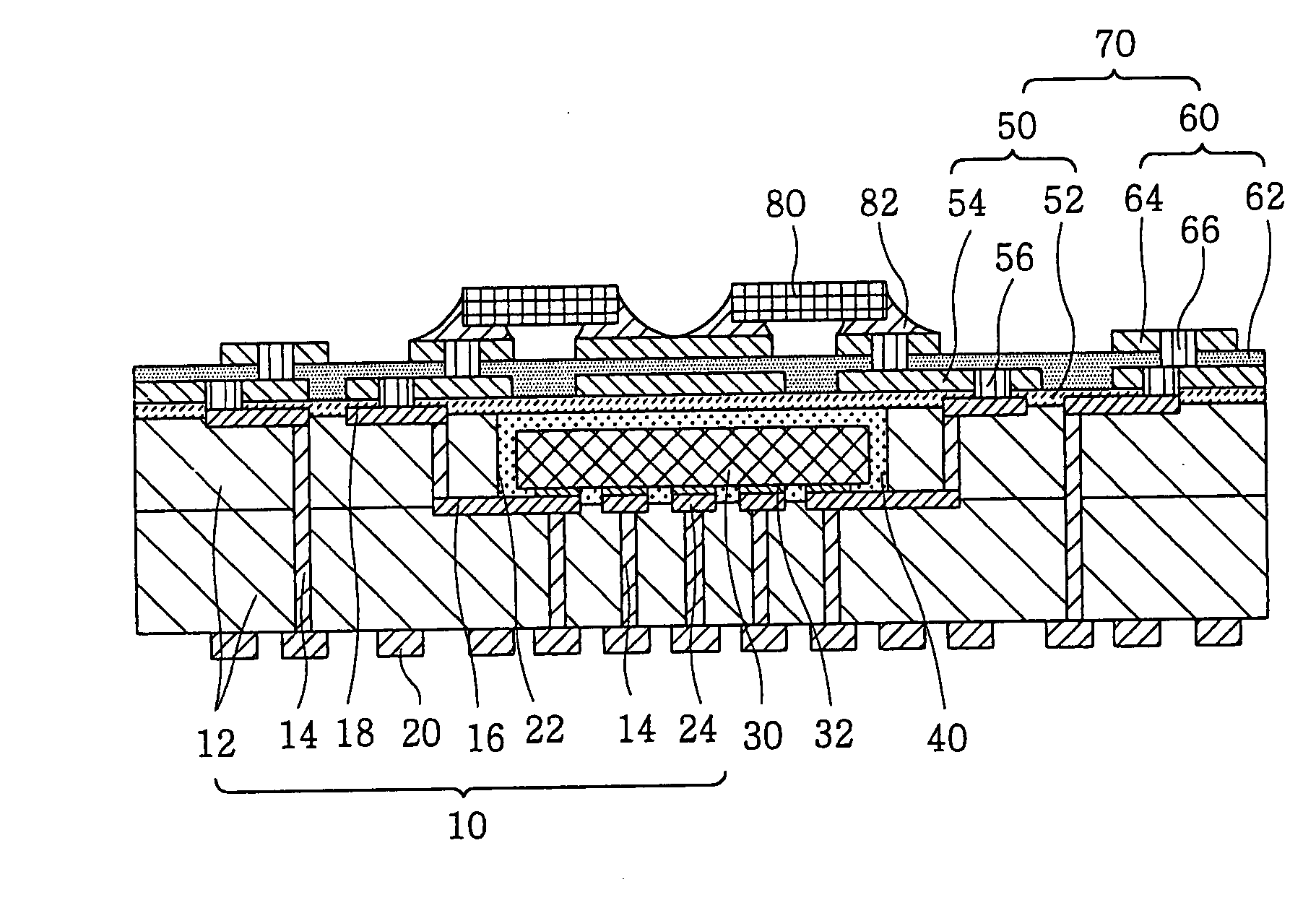
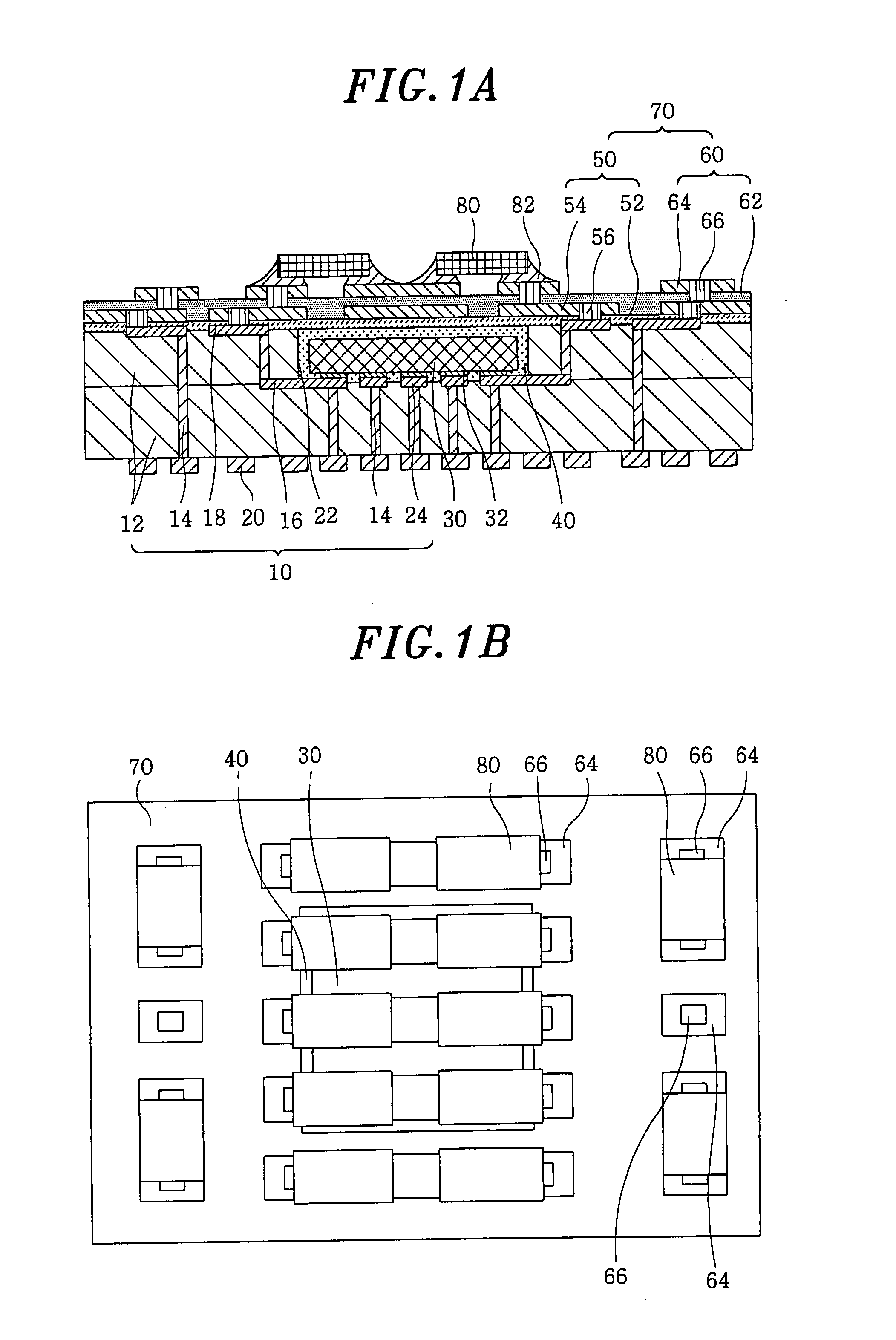
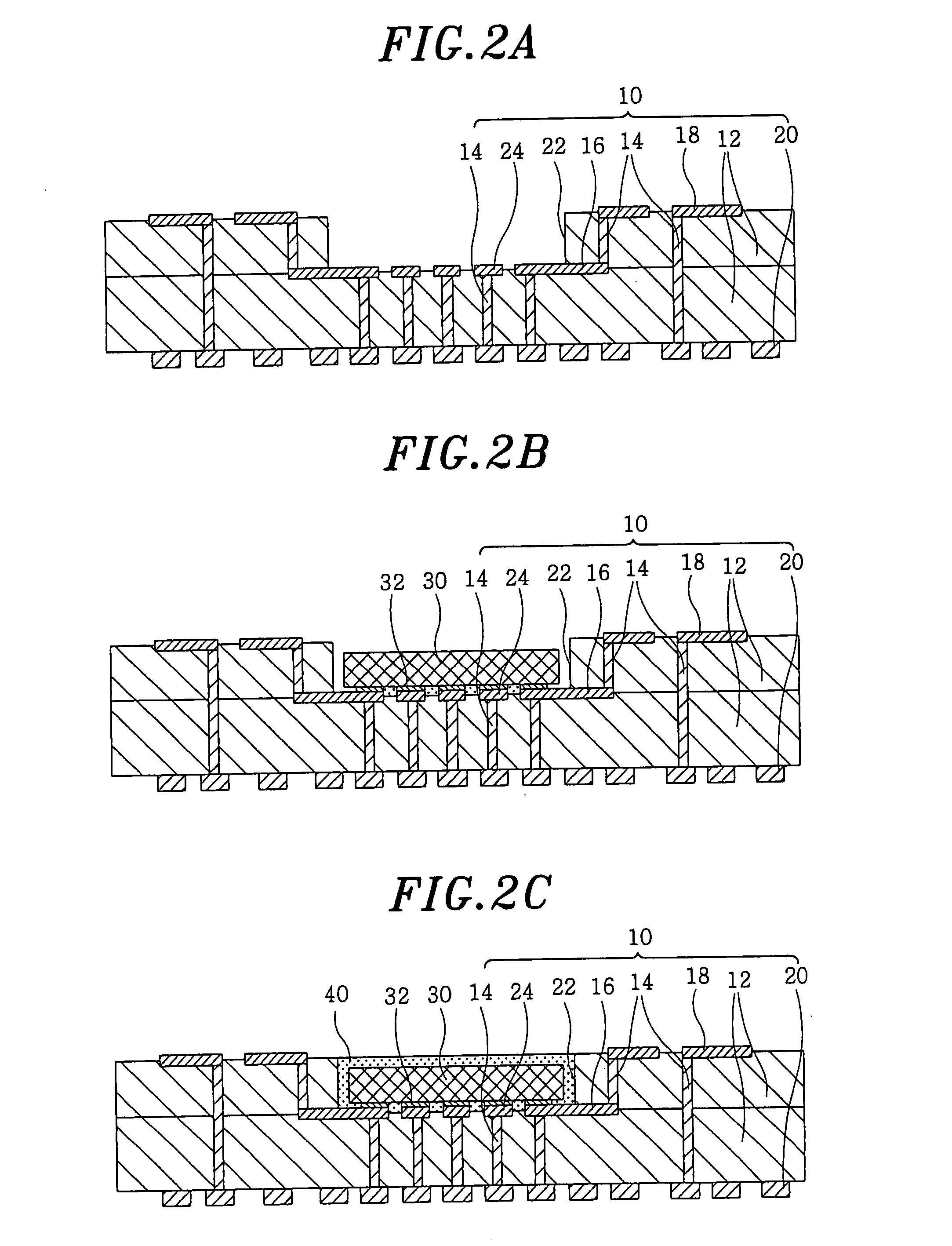
[0050] A circuit module and a method of manufacturing same, in accordance with a first embodiment of this invention, are described with reference to FIGS. 1A to 4B.

[0051]FIGS. 1A and 1B are a cross-sectional view and a top plan view, respectively, of a circuit module in accordance with this first embodiment.

[0052] Multilayer ceramic substrate 10 is provided with conductive via 14 formed in dielectric layer 12 to make electrical connection between layers; interior wiring layer 16, top surface wiring layer 18 and bottom surface wiring layer 20, all of which are electrically connected with conductive via 14; and cavity 22 for mounting electronic component 30 thereon. For such multilayer ceramic substrate 10, for instance, when a glass-ceramic material is used as dielectric layers 12, it can be sintered at a relatively low temperature in the range of about 900-1000° C. Consequently, dielectric layers 12 can be co-sintered with materials that form conductive via 14 and interior wiring ...

second embodiment

[0080]FIGS. 7A to 7C are cross-sectional views illustrating a process of fabricating sheet 500 in the method of fabricating a circuit module in accordance with a second embodiment of the present invention. Further, FIGS. 8A and 8B are cross-sectional views showing a process of stacking sheet 500 on ceramic multilayer substrate 10 wherein IC 30 is mounted on cavity 22 and the substrate is planarized by using thermosetting resin 40, ultimately forming a first wiring layer 540.

[0081] The second embodiment is different from the first embodiment with respect to the processes of fabricating sheet 500 and of forming first wiring layer 540 after stacking sheet 500 on ceramic multilayer substrate 10. Hereinafter, a method of fabricating a circuit module is described while focusing on its differences with the first embodiment.

[0082] As shown in FIG. 7A, using sheet 500 composed of first metal layer 542 (e.g., copper film) and first insulating adhesive layer 521, first opening 562 is formed ...

third embodiment

[0089]FIGS. 10A to 10D are cross-sectional views illustrating a process of fabricating sheet 510 in the method of fabricating a circuit module in accordance with a third embodiment of the present invention. Further, FIG. 11 is a cross-sectional view showing a process of stacking sheet 510 having first wiring layer 545 formed thereon, on ceramic multilayer substrate 10 wherein IC 30 is mounted on cavity 22 and the substrate is planarized using thermosetting resin 40.

[0090] In this embodiment, with respect to the fabricating step of sheet 510, its difference with that of the first embodiment lies in its stacking step on ceramic multilayer substrate 10 which is carried out after first wiring layer 545 is formed. Hereinafter, a method of fabricating a circuit module is described while focusing on its differences with the first embodiment.

[0091] As shown in FIG. 10A, using sheet 510 composed of first metal layer 544 (e.g., copper film) and first insulating adhesive layer 522, first ope...


PUM


Abstract

A circuit module includes an electronic component, a ceramic multilayer substrate and a resin wiring substrate. The ceramic multilayer substrate is provided with a wiring layer disposed on top thereof and a cavity in which the electronic component is mounted, wherein a space between the electronic component and the cavity is filled with a thermosetting resin and a surface of the filled cavity is planarized. The resin wiring substrate has an insulating adhesive layer disposed at one side thereof and provided with at least one opening filled with a conductive resin. The ceramic multilayer substrate and the resin wiring substrate are bonded by the insulating adhesive layer, and the wiring layer on the ceramic multilayer substrate is electrically connected with the conductive resin.

Description

[0001] This application is a divisional application of pending U.S. application Ser. No. 10 / 895,050 filed Jul. 21, 2004.FIELD OF THE INVENTION [0002] The present invention relates to a high-performance circuit module having electronic components such as a semiconductor integrated circuit (hereinafter, refer to as an “IC”) and a manufacturing method thereof. BACKGROUND OF THE INVENTION [0003] Along with a high density integration and a high speed performance of ICs, concerted efforts are being made to develop technologies to increase the number of terminals and to narrow the pitches of a package on which such an IC is mounted. With respect to this, a technological progress is underway to fabricate a circuit module, on which electronic devices such as an IC is mounted, that is larger in scale, faster in speed, and smaller in size. In order to achieve such a miniaturization and high density of a circuitry, it is required to increase the number of wiring layers, to miniaturize wirings, ...

Claims


Application Information

Patent Timeline
Patent Type & Authority Applications(United States)
IPC IPC(8): H01L21/50H01L23/13H01L23/24H01L23/538H01L25/00H01L25/065H01L25/07H01L25/18H05K1/03H05K1/18H05K3/38H05K3/40H05K3/46
CPCH01L23/24H01L2924/01322H01L2224/16225H01L2924/01046H01L2924/01078H01L2924/01079H01L2924/09701H01L2924/15153H01L2924/1517H05K1/0306H05K1/186H05K3/386H05K3/4069H05K3/4605H05K3/4614H05K3/4617H05K3/4629H05K3/4652H05K2203/061H01L2924/01019H01L23/5389
Inventor MORIMOTO, KENJISEGAWA, SHIGETOSHI
Owner PANASONIC CORP
Why Eureka
Try Eureka