

Circuit Substrate and Method
- Summary
- Abstract
- Description
- Claims
- Application Information
AI Technical Summary
Benefits of technology
Problems solved by technology
Method used
Image

Examples
Example
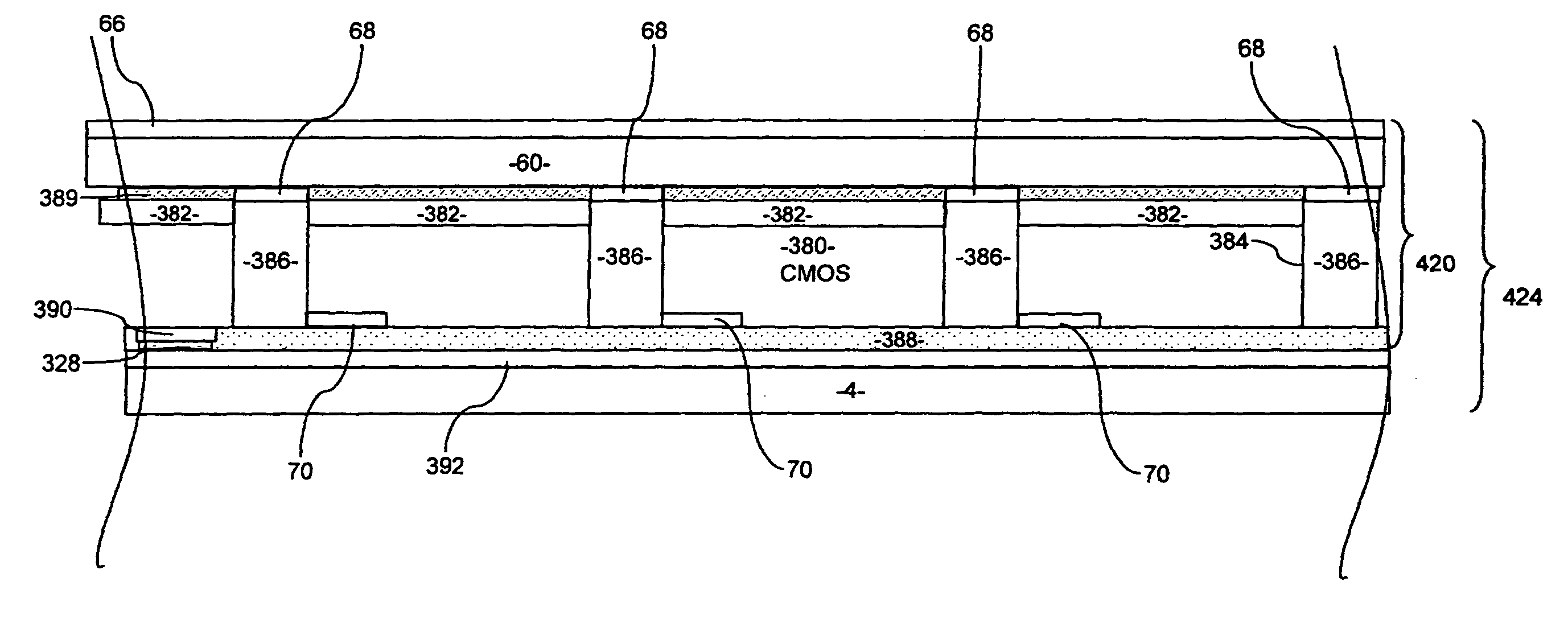
[0069]FIG. 5 illustrates a first embodiment in accordance with one aspect of the invention, comprising an imaging device 320 formed of a detector substrate 60 having a detector cell contact 68 flip chip bonded to a cell circuit substrate 362 (the flip chip bond is shown in exploded form for clarity). The detector substrate 60 is flip chip-bonded to the circuit substrate 362 via bump bonds 64 which are built on circuit contacts of cell circuits 70. Whilst in FIG. 5 the control signal, readout signal and supply voltage lines 361 for the circuit substrate 362 are arranged so that they terminate in a region at one end, 326, of the circuit substrate 362, they could alternatively be located at any region within the circuit substrate.
[0070]A series of via holes 321 forming signal pathways are etched through the circuit substrate 362 in the region 326 so as to provide a conduit between respective surfaces of substrate 362. Contact pads 322a and 322b may be formed on respective surfaces of t...
PUM
 Abstract
Description
Claims
Application Information