Light emission device and display device

a technology of light emission device and display device, which is applied in the direction of discharge tube main electrode, discharge tube luminescnet screen, discharge tube with screen, etc., can solve the problems of increasing the dead space of the substrate, the above-described anode voltage applying structure of the above-described light emission device, etc., to avoid damage to the substrate, reduce (or minimize) the dead space, and enhance the effect of dynamic contras

Inactive Publication Date: 2008-04-24
SAMSUNG SDI CO LTD
View PDF8 Cites 9 Cited by
  • Summary
  • Abstract
  • Description
  • Claims
  • Application Information

AI Technical Summary

Benefits of technology

[0010]Aspects of exemplary embodiments of the present invention are directed to a light emission device that can avoid damage to a substrate while also reducing (or minimizing) a dead space (e.g., an inactive region of the light emission device).
[0011]Aspects of exemplary embodiments of the present invention are directed to a light emission device that has a light emission surface divided into a plurality of regions and that can independently control a light emission intensity of each divided region, and a display device that can enhance a dynamic contrast by employing the light emission device.

Problems solved by technology

Therefore, the anode voltage applying structure of the above-described light emission device has a drawback because it increases a dead space of the substrate.

Method used


Image

  • Light emission device and display device
  • Light emission device and display device
  • Light emission device and display device

Examples


Embodiment Construction

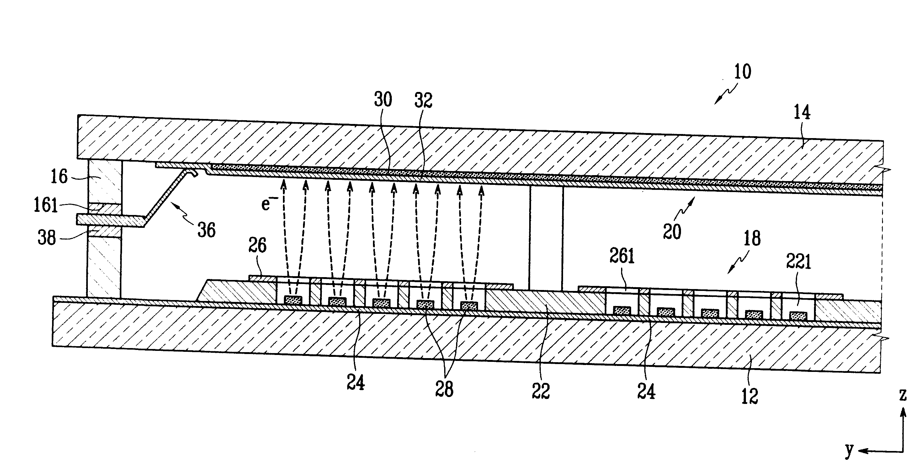
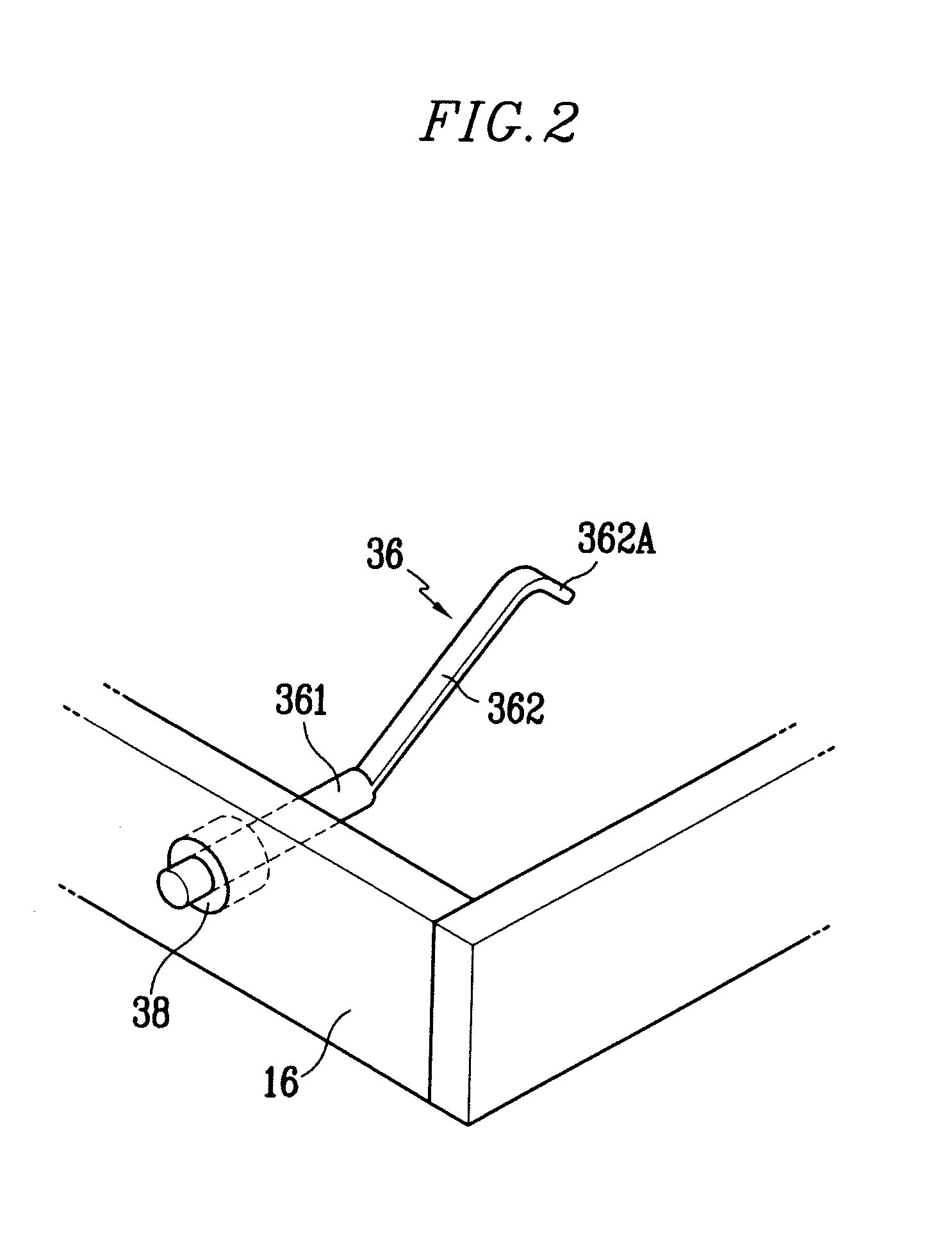
[0023]In the following detailed description, only certain exemplary embodiments of the present invention have been shown and described, simply by way of illustration. As those skilled in the art would realize, the described embodiments may be modified in various different ways, all without departing from the spirit or scope of the present invention. Accordingly, the drawings and description are to be regarded as illustrative in nature and not restrictive. Also, in the context of the present application, when an element is referred to as being “on” another element, it can be directly on the another element or be indirectly on the another element with one or more intervening elements interposed therebetween. Like reference numerals designate like elements throughout the specification.

[0024]A light emission device of certain exemplary embodiments can be construed as a light source of a display device (e.g., a non-self-emissive display device such as a liquid crystal display, etc.) or a...


PUM


Abstract

A light emission device and a display device provided with the light emission device. The light emission device includes first and second substrates opposing each other; a side member located between periphery regions of the first and second substrates to define a vacuum chamber with the first and second substrates; an electron emission unit disposed on the first substrate; and a light emission unit disposed on the second substrate and adapted to emit light using electrons emitted from the electron emission unit. The light emission unit includes a phosphor layer and an anode electrode disposed on a surface of the phosphor layer, and the anode electrode is applied with a voltage through an anode terminal penetrating through the side member.

Description

CROSS-REFERENCE TO RELATED APPLICATION[0001]This application claims priority to and the benefit of Korean Patent Application No. 10-2006-0102907, filed on Oct. 23, 2006, in the Korean Intellectual Property Office, the entire content of which is incorporated herein by reference.BACKGROUND OF THE INVENTION[0002]1. Field of the Invention[0003]The present invention relates to a light emission device and a display using the light emission device as a light source.[0004]2. Description of Related Art[0005]A liquid crystal display is an example of a passive type display device (or non-self-emissive display device) requiring a light source. The liquid crystal display includes a display panel having a liquid crystal layer and a polarizer plate and a light emission device for emitting light toward the display panel. The display panel receives the light from the light emission device and selectively transmits or blocks the light using the liquid crystal layer and the polarizing plate, thereby d...

Claims


Application Information

Patent Timeline
Patent Type & Authority Applications(United States)
IPC IPC(8): H01J1/62
CPCC09K11/06C09K2211/1007C09K2211/1014H05B33/14C09K2211/1037H01J29/085H01J31/127C09K2211/1029H01J1/30H01J31/12
Inventor RYU, KYUNG-SUNWON, YONG-GUN
Owner SAMSUNG SDI CO LTD
Why Eureka
Try Eureka