Chip-Shaped Electronic Part

a technology of electronic parts and chips, applied in the manufacture of resistor chips, resistor details, resistors, etc., can solve problems such as serious cracks in substrates, and achieve the effect of suppressing cracks in substrates

Active Publication Date: 2008-04-24
PANASONIC CORP
View PDF3 Cites 21 Cited by
  • Summary
  • Abstract
  • Description
  • Claims
  • Application Information

AI Technical Summary

Benefits of technology

[0016] In order to solve the above-mentioned conventional disadvantages, it is an object of the invention to provide a chip-shaped electronic part that enables to suppress crack...

Problems solved by technology

In particular, the substrate crack is serious, if the substrate 1 with a small thickness is used in the small-sized chip-shaped electroni...

Method used


Image

  • Chip-Shaped Electronic Part
  • Chip-Shaped Electronic Part
  • Chip-Shaped Electronic Part

Examples


first embodiment

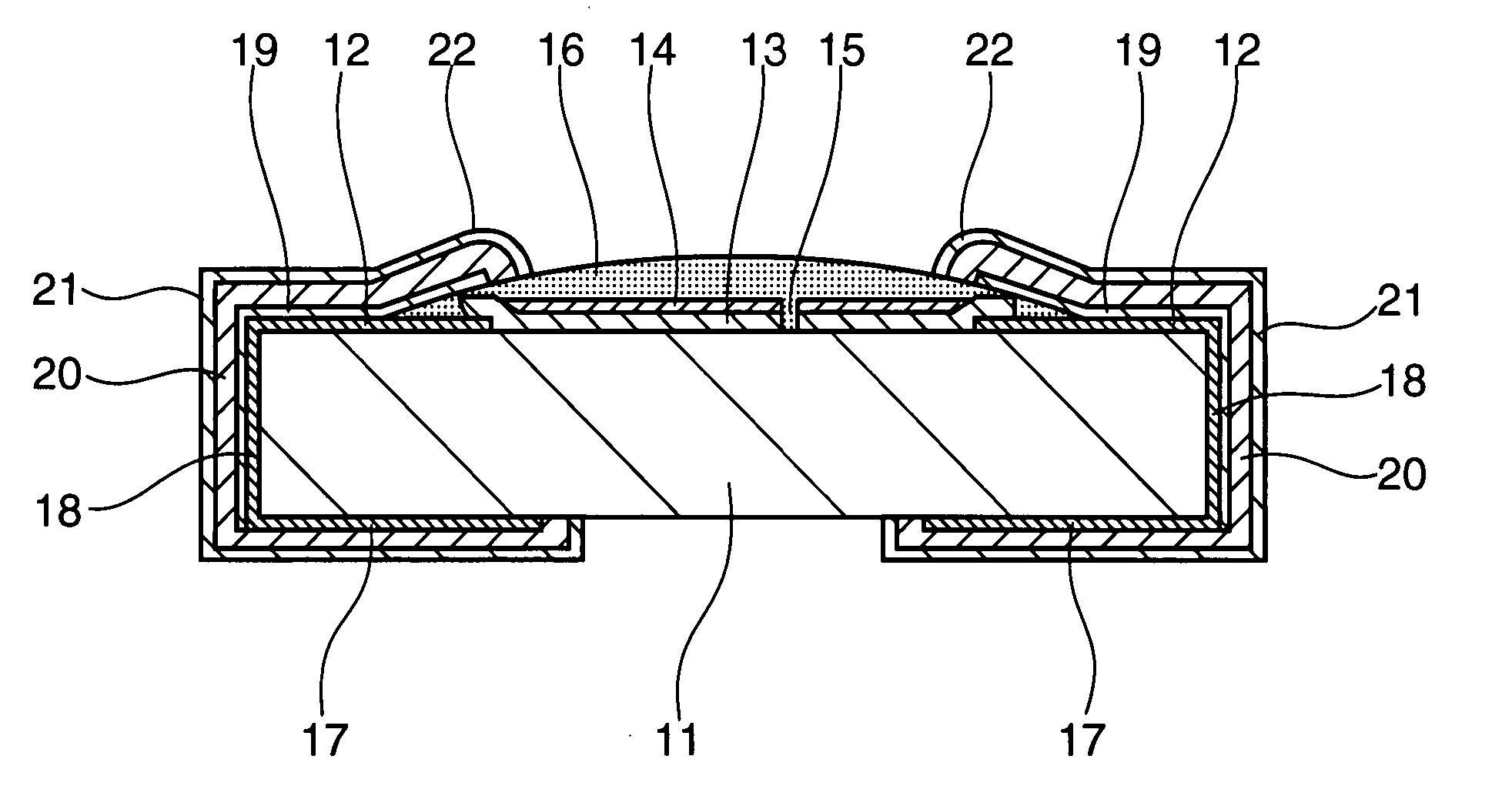
[0035]FIG. 1 is a cross-sectional view showing a chip resistor, as an example of a chip-shaped electronic part according to the first embodiment of the invention. A substrate 11 is made of ceramics such as fired alumina, and has an insulation property. The thickness of the substrate 11 is decreased, as the size of the chip-shaped electronic part is decreased. For instance, a substrate 11 of a 0603 chip resistor with the outer dimensions of 0.6 mm×0.3 mm has a standard thickness of 0.2 mm, and a substrate 11 of a 0402 chip resistor with the outer dimensions of 0.4 mm×0.2 mm has a standard thickness of 0.1 mm.

[0036] A pair of first upper surface electrodes 12 are formed at widthwise both ends on an upper surface of the substrate 11. The first upper surface electrode pair 12 is made of a gold resinate paste containing gold. A ruthenium-oxide-based resistive element 13 is formed on the upper surface of the substrate 11 in such a manner that both ends thereof are placed over the first u...

second embodiment

[0069]FIG. 6 is a cross-sectional view showing a chip resistor, as an example of a chip-shaped electronic part according to the second embodiment of the invention. A substrate 31 is made of ceramics such as fired alumina, and has an insulation property. The thickness of the substrate 31 is decreased, as the size of the chip-shaped electronic part is decreased. For instance, a substrate 31 of a 0603 chip resistor with the outer dimensions of 0.6 mm×0.3 mm has a standard thickness of 0.2 mm, and a substrate 31 of a 0402 chip resistor with the outer dimensions of 0.4 mm×0.2 mm has a standard thickness of 0.1 mm.

[0070] A pair of upper surface electrodes 32 are formed at widthwise both ends on an upper surface of the substrate 31. The upper surface electrode pair 32 is made of a gold resinate paste containing gold, and has a thickness of about 1 μm. A ruthenium-oxide-based resistive element 33 is formed on the upper surface of the substrate 31 in such a manner that both ends thereof are...

third embodiment

[0097]FIG. 10 is a cross-sectional view showing a chip resistor, as an example of a chip-shaped electronic part according to the third embodiment of the invention. The third embodiment is a combination of the second embodiment and a modification of the first embodiment. Elements in the third embodiment identical or equivalent to those in the second embodiment are denoted at the same reference numerals as the second embodiment.

[0098] Specifically, an upper surface of a protective film 36 is made substantially flat by setting the thickness of a portion of the protective film 36 above a resistive element 33 to 7 μm or less. Also, the thicknesses of a first plated layer 39 and a second plated layer 40 are set so that the height from the upper surface 31 to the upper surface of the second plated layer 40 is in the range from 12 μm to 21 μm, and is larger than the height from the upper surface of the substrate 31 to the upper surface of the protective film 36 i.e. from 10 μm to 14 μm; an...


PUM


Abstract

A chip-shaped electronic part includes: a substrate; a pair of upper surface electrodes formed on an upper surface of the substrate; a functional element formed to be electrically connected to the upper surface electrode pair; a pair of lower surface electrodes formed on a lower surface of the substrate at positions opposing the upper surface electrode pair; a pair of end surface electrodes formed on end surfaces of the substrate so that each of the end surface electrode pair is electrically connected to one of the upper surface electrode pair, and to one of the lower surface electrode pair corresponding to the one upper surface electrode; a protective film formed in such a manner as to cover at least the functional element; and a plated layer formed in such a manner as to cover at least each of the upper surface electrode pair, wherein the protective film or the plated layer has at least two points of application at which a load from above the substrate is exerted.

Description

TECHNICAL FIELD [0001] The present invention relates to a chip-shaped electronic part adapted for various electronic devices. BACKGROUND ART [0002] Hereinafter, a conventional chip-shaped electronic part is described referring to the drawings. [0003]FIG. 11 is a cross-sectional view of a chip resistor, as an example of the conventional chip-shaped electronic part. A substrate 1 is made of ceramics such as alumina, and has an insulation property. The thickness of the substrate 1 is decreased, as the size of the chip-shaped electronic part is decreased. For instance, a substrate 1 of a 0603 chip resistor with the outer dimensions of 0.6 mm×0.3 mm has a standard thickness of 0.2 mm, and a substrate 1 of a 0402 chip resistor with the outer dimensions of 0.4 mm×0.2 mm has a standard thickness of 0.1 mm. [0004] A pair of upper surface electrodes 2 are formed at widthwise both ends on an upper surface of the substrate 1. The upper surface electrode pair 2 generally has a film thickness of ...

Claims


Application Information

Patent Timeline
IPC IPC(8): H01C1/142H05K7/02
CPCH01C1/06H01C17/006H01C7/003H01C1/142
Inventor KINOSHITA, YASUHARUMATSUKAWA, TOSHIKISHIBUYA, NAOKIHOSHITOKU, SHOJI
Owner PANASONIC CORP
Why Eureka
Try Eureka