Solid-state image pickup device and image pickup apparatus
- Summary
- Abstract
- Description
- Claims
- Application Information
AI Technical Summary
Benefits of technology
Problems solved by technology
Method used
Image
Examples
Embodiment Construction
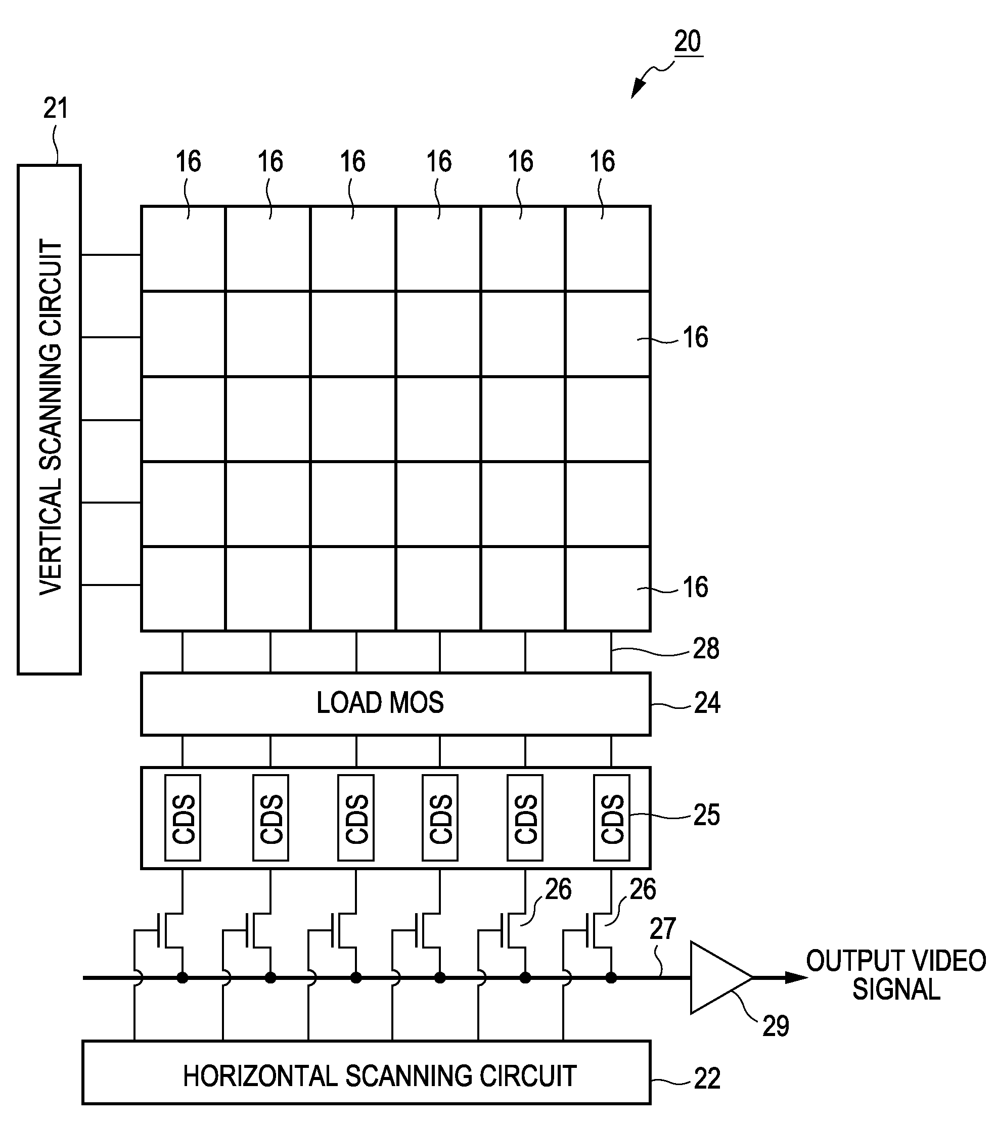
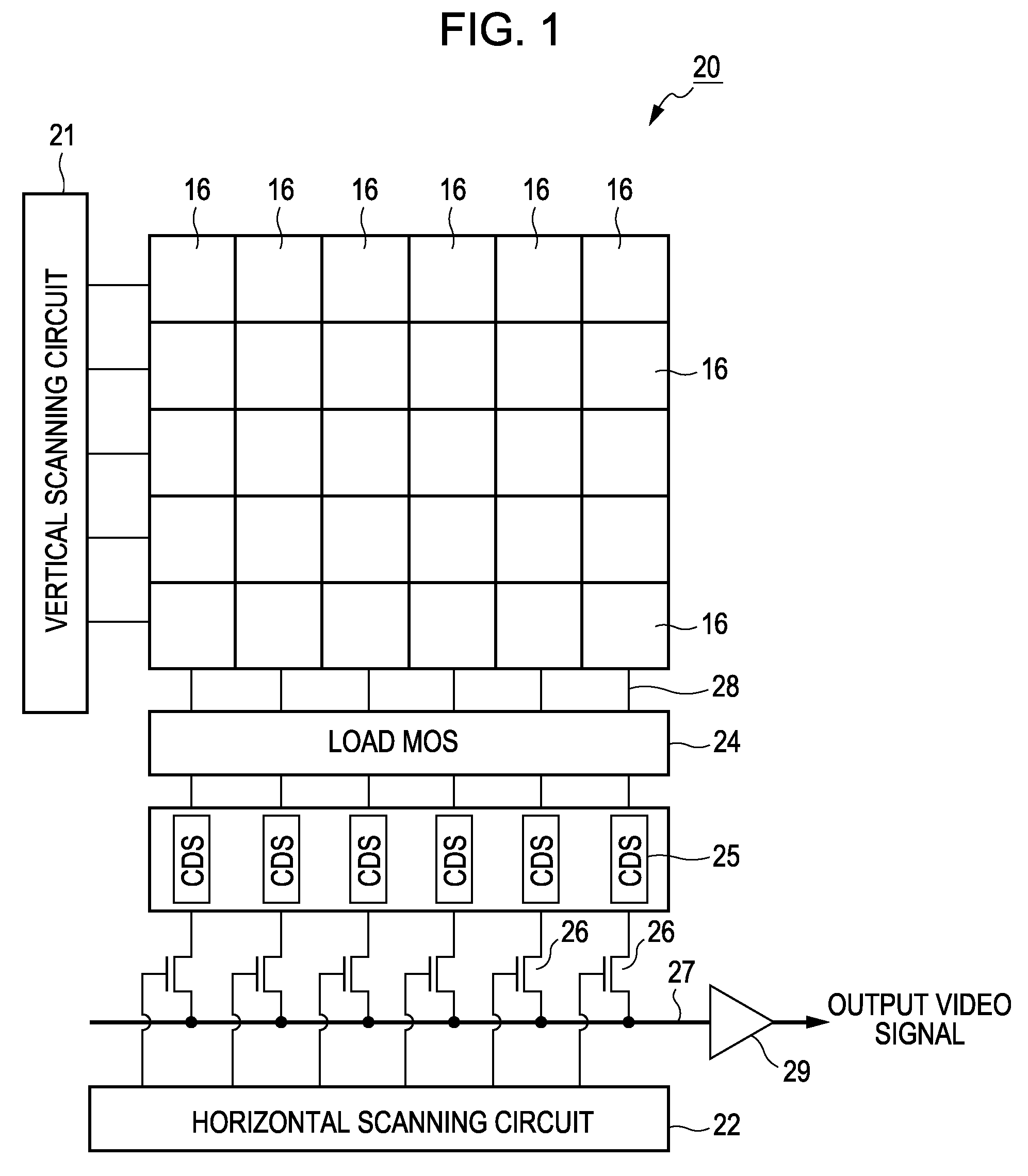
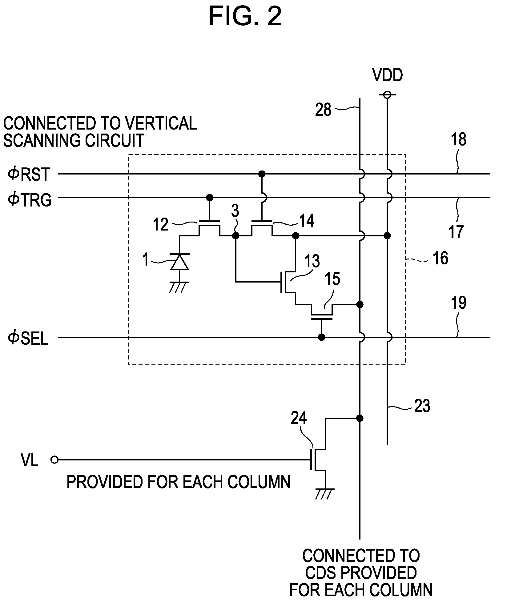
[0026]FIG. 1 is a plan view illustrating a CMOS image sensor as an example of a solid-state image pickup device according to an embodiment of the present invention. FIG. 2 is a circuit diagram illustrating a circuit configuration in a pixel of the solid-state image pickup device illustrated in FIG. 1.
[0027]FIG. 3 is a block diagram illustrating an exemplary configuration of a digital clamp correction circuit, which is provided for correcting an optical black (OB) signal to a target value in a signal processing circuit of the solid-state image pickup device according to the present embodiment.
[0028]Although a CMOS image sensor will be primarily described in the following embodiments, the present invention is similarly applicable to a CCD image sensor.
[0029]As illustrated in FIG. 1, a solid-state image pickup device of the present embodiment includes a pixel array unit 20, a vertical scanning circuit 21, a load metal oxide semiconductor (MOS) transistor circuit 24, correlated double s...
PUM
 Abstract
Description
Claims
Application Information


