Semiconductor device having electrostatic protection circuit
- Summary
- Abstract
- Description
- Claims
- Application Information
AI Technical Summary
Benefits of technology
Problems solved by technology
Method used
Image
Examples
first embodiment
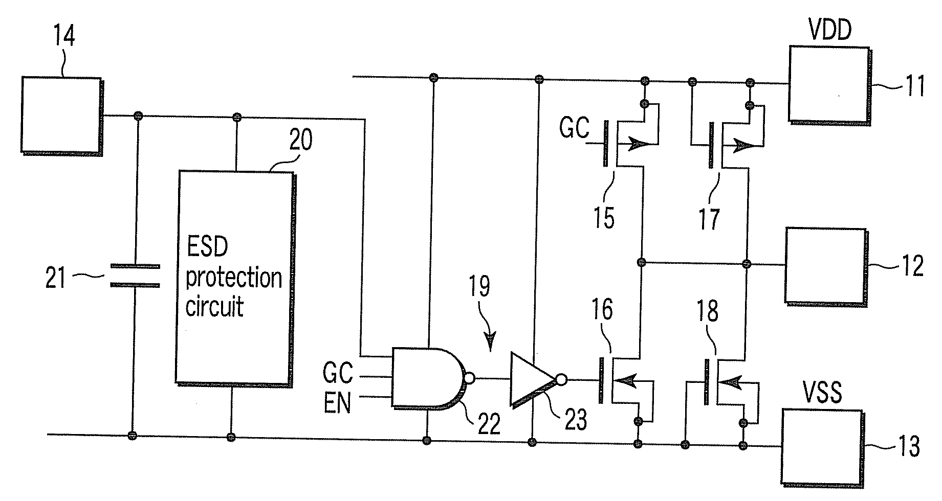
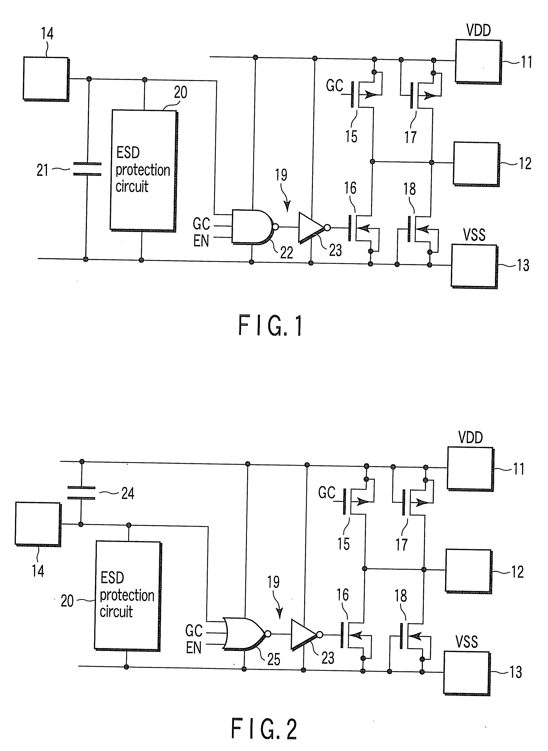
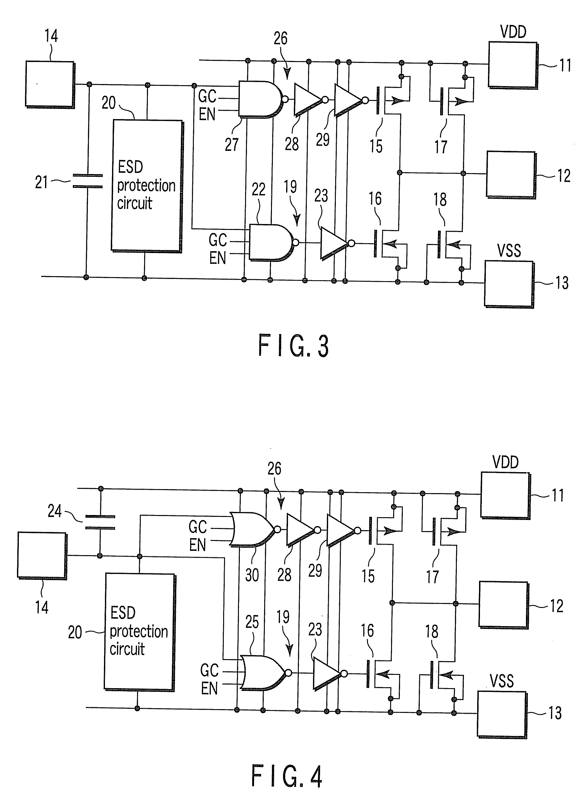
[0030]FIG. 1 is a circuit diagram showing an electrostatic protection circuit and its peripheral circuits so as to explain a semiconductor device according to the first embodiment of the present invention. FIG. 1 places focus on an output buffer. This circuit includes a power supply terminal (VDD terminal) 11, I / O terminal 12, reference potential terminal (VSS terminal) 13, external input terminal 14, buffer PMOSFET 15, buffer NMOSFET 16, SGPMOSFET 17, GGNMOSFET 18, prebuffer 19, ESD protection circuit 20, and capacitive element 21.
[0031]A power supply potential VDD is applied to the power supply terminal (power supply pad) 11. A reference potential VSS is applied to the reference potential terminal (reference potential pad) 13. The I / O terminal (I / O pad) 12 inputs / outputs data. The buffer PMOSFET 15 and buffer NMOSFET 16 form an output buffer. The current path between the source and drain of the buffer PMOSFET 15 is connected between the power supply terminal 11 and the I / O termina...
second embodiment
[0055]FIG. 5 is a circuit diagram showing an electrostatic protection circuit and its peripheral circuits so as to explain a semiconductor device according to the second embodiment of the present invention. FIG. 5 places focus on an output buffer, as in the first embodiment. This circuit includes a power supply terminal (VDD terminal) 31, I / O terminal 32, reference potential terminal (VSS terminal) 33, external input terminal 34, buffer PMOSFET 35, buffer NMOSFET 36, prebuffer 37, ESD protection circuits 38 and 39, and capacitive element 40.
[0056]A power supply potential VDD is applied to the power supply terminal 31. A reference potential VSS is applied to the reference potential terminal 33. The I / O terminal 32 inputs / outputs data. The buffer PMOSFET 35 and buffer NMOSFET 36 form an output buffer. The current path between the source and drain of the buffer PMOSFET 35 is connected between the power supply terminal 31 and the I / O terminal 32 to pull up the I / O terminal 32 to the pow...
first modification
(First Modification)
[0068]FIG. 7 is a circuit diagram showing an electrostatic protection circuit and its peripheral circuits so as to explain a first modification of the semiconductor device according to the second embodiment of the present invention. In the second embodiment, the external input terminal 34 capacitively couples to the reference potential terminal 33 via the capacitive element 40. In the first modification, the external input terminal 34 capacitively couples to the power supply terminal 31 via a capacitive element 51. In the normal operation mode, the reference potential VSS is applied to the external input terminal 34. Additionally, a 3-input NOR circuit 52 is provided in place of the 3-input NAND circuit 41.
[0069]The remaining basic components are the same as in the second embodiment. The same reference numerals as in the second embodiment denote the same parts in this modification, and a detailed description thereof will not be repeated.
[0070]According to the abo...
PUM
 Abstract
Description
Claims
Application Information


