Techniques for reducing a voltage swing

a technology of random access memory and voltage swing, which is applied in the direction of information storage, static storage, digital storage, etc., can solve the problems of large power consumption, disruption of memory cells on unselected rows, and over-majority charge carriers, so as to reduce voltage swing and reduce voltage swing

Active Publication Date: 2011-04-26
MICRON TECH INC
View PDF385 Cites 178 Cited by
  • Summary
  • Abstract
  • Description
  • Claims
  • Application Information

AI Technical Summary

Problems solved by technology

Also, conventional writing techniques for memory cells having an N-Channel type memory transistor typically result in an excess of majority charge carriers by channel impact ionization or by band-to-band tunneling (gate-induced drain leakage “GIDL”).
Often, conventional reading and writing techniques may lead to relatively large power consumption and large voltage swings which may cause disruptions to memory cells on unselected rows.
However, some of the minority charge carriers may remain “trapped” in interface defects.
This phenomenon may be characterized as charge pumping, which is a problem because the net quantity of charge carriers may be reduced in the memory cell, which, in turn, may gradually eliminate data stored in the memory cell.
In view of the foregoing, it may be understood that there are significant problems and shortcomings associated with reading from and / or writing to semiconductor dynamic random access memory (“DRAM”) devices using conventional current sensing technologies.

Method used


Image

  • Techniques for reducing a voltage swing
  • Techniques for reducing a voltage swing
  • Techniques for reducing a voltage swing

Examples


Embodiment Construction

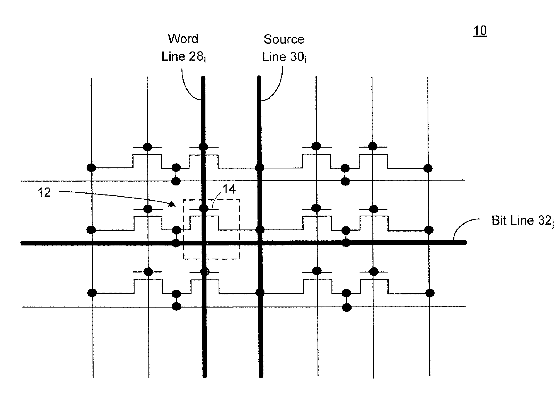
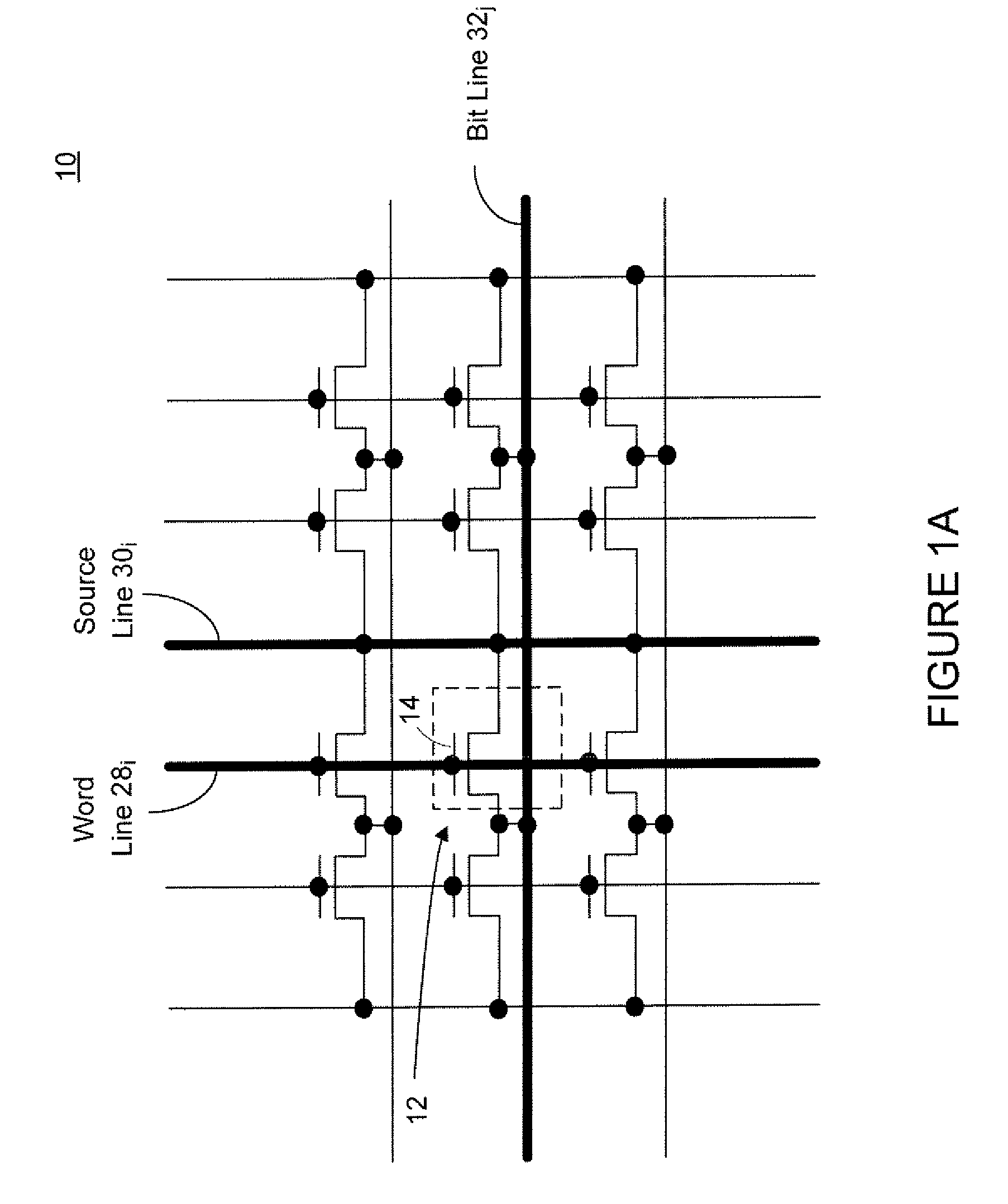
[0053]There are many embodiments described and illustrated herein. In one aspect, the present disclosure is directed to a combination of reading / writing methods which allows relatively low power consumption and provides a relatively low voltage swing and thus reduces disruptions to unselected memory cells.

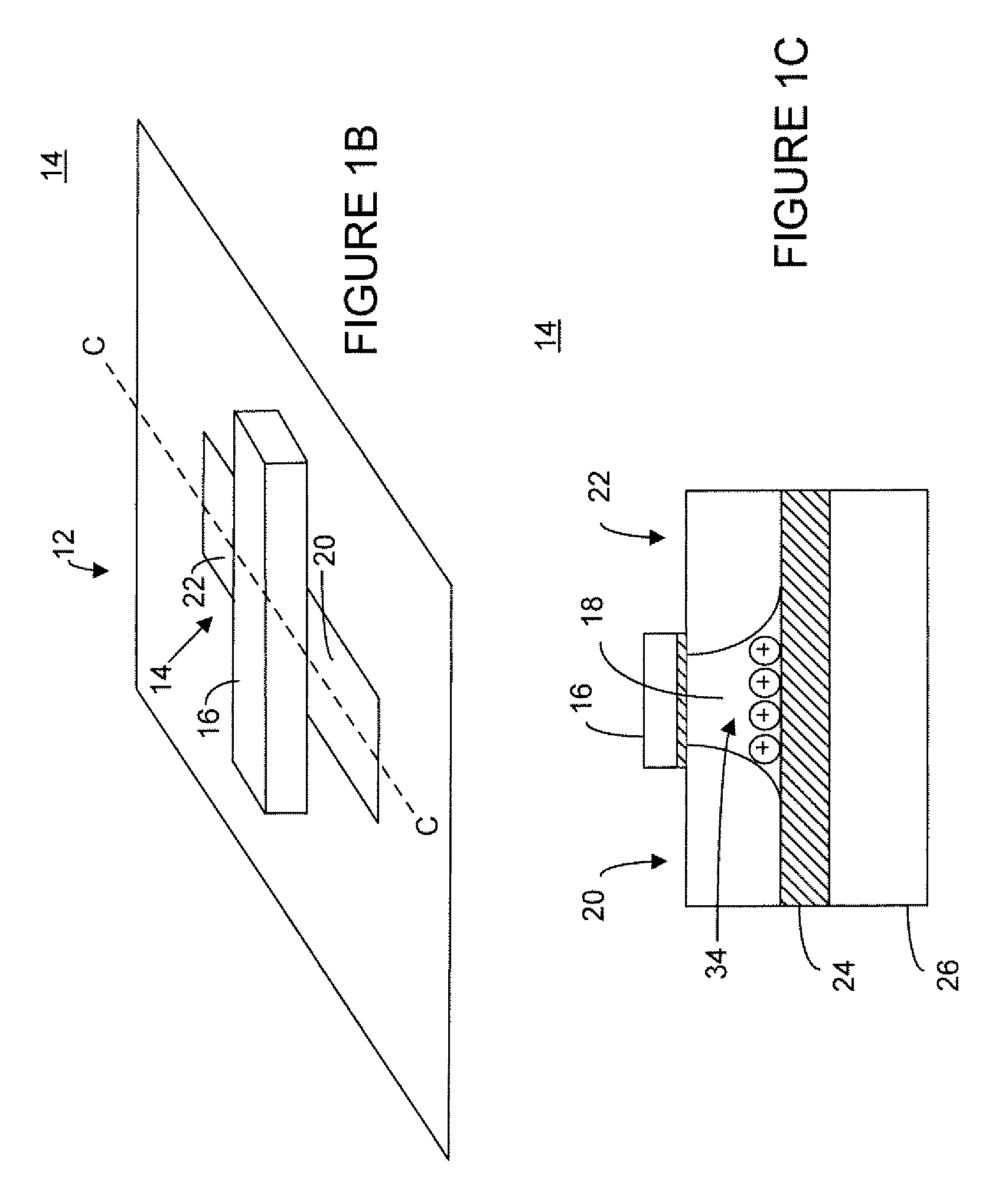
[0054]Referring to FIGS. 1A, 1B, and 1C, a semiconductor DRAM device 10 (e.g., a logic or discrete memory device) including one or more memory cells 12 including a memory transistor 14 having an electrically floating body (e.g., an N-channel type transistor or a P-channel type transistor). The memory transistor 14 includes a source region 20, a drain region 22, a body region 18 disposed between the source region 20 and the drain region 22, wherein the body region 18 is electrically floating, and a gate 16 disposed over the body region 18. Moreover, the body region 18 may be disposed on or above region 24, which may be an insulation region (e.g., in an SOT material / substrate) or non...


PUM


Abstract

Techniques for reducing a voltage swing are disclosed. In one particular exemplary embodiment, the techniques may be realized as an apparatus for reducing a voltage swing comprising: a plurality of dynamic random access memory cells arranged in arrays of rows and columns, each dynamic random access memory cell including one or more memory transistors. The one or more memory transistors of the apparatus for reducing a voltage swing may comprise: a first region coupled to a source line, a second region coupled to a bit line, a first body region disposed between the first region and the second region, wherein the first body region may be electrically floating, and a first gate coupled to a word line spaced apart from, and capacitively coupled to, the first body region. The apparatus for reducing a voltage swing may also comprise a first voltage supply coupled to the source line configured to supply a first voltage and a second voltage to the source line, wherein a difference between the first voltage and the second voltage may be less than 3.5V.

Description

FIELD OF THE DISCLOSURE[0001]The present disclosure relates generally to semiconductor dynamic random access memory (“DRAM”) devices and, more particularly, to techniques for reducing a voltage swing in a semiconductor dynamic random access memory (“DRAM”) device.BACKGROUND OF THE DISCLOSURE[0002]There is a continuing trend to employ and / or fabricate advanced integrated circuits using techniques, materials, and devices that improve performance, reduce leakage current, and enhance overall scaling. Semiconductor-on-insulator (SOI) is a material which may be used to fabricate such integrated circuits. Such integrated circuits are known as SOI devices and may include, for example, partially depleted (PD) devices, fully depleted (FD) devices, multiple gate devices (for example, double or triple gate), and Fin-FET devices.[0003]A semiconductor dynamic random access memory (“DRAM”) device may include an electrically floating body in which electrical charges may be stored. The electrical ch...

Claims


Application Information

Patent Timeline
Patent Type & Authority Patents(United States)
IPC IPC(8): G11C11/24
CPCG11C11/404G11C11/4085G11C11/4074G11C2211/4016
Inventor WANG, PINGCARMAN, ERIC
Owner MICRON TECH INC
Why Eureka
Try Eureka