Integrated circuit devices and methods and apparatuses for designing integrated circuit devices

a technology of integrated circuits and circuits, applied in the field of integrated circuit devices, can solve the problems of increasing the difficulty of capacitive and inductive coupling of signal lines within the circuitry itself, the difficulty of particular issue of capacitive and inductive coupling in signals, and the realization of critical problems for designers. the effect of temperature variation

Active Publication Date: 2006-05-04
SYNOPSYS INC
View PDF18 Cites 189 Cited by
  • Summary
  • Abstract
  • Description
  • Claims
  • Application Information

AI Technical Summary

Benefits of technology

[0014] Methods and apparatuses to design an Integrated Circuit (IC) with a shielding of wires of at least two different voltages are described here. In one aspect of the invention, an exemplary method for designing an integrated circuit includes determining at least one temperature of an integrated circuit and inserting, in response to the determining, a representation of a shielding mesh into at least one layer of the integrated circuit. In one implementation of this method, a plurality of temperatures may be determined at a plurality of different locations on the integrated circuit. This plurality of temperatures represents a temperature profile, and the shielding mesh is capable of reducing a variation of temperatures in the temperature profile.

Problems solved by technology

However, when the semiconductor industry designs and implements circuitry based on the sub-micron level technology and beyond, where spacing between circuitry lines is less than 10-6 microns, the capacitive and inductive coupling of the signal lines within the circuitry itself is realized to be a critical problem for designers.
As circuit size becomes smaller and the lengths of signal lines become longer relative to the width of the lines, the problem of coupling and / or cross talk between signal lines and ground or power lines becomes more evident.
This particular issue of capacitive and inductive coupling in signals is becoming increasingly difficult as the industry advances and moves towards reduction in circuit device size (for example, from 0.25 micron technology to 0.18 micron, 0.15 micron, 0.13 micron and beyond).
Unfortunately, to increase the signal strength, the device must also be supplied with higher power, which is inconsistent with the requirement of reducing power consumption in ICs for heat issues, portability issues and environmental issues.
In addition to the higher power consumption, increasing the signal strength does not eliminate signal coupling.
The signal of increased strength may cause increased noise in the adjacent signal lines through capacitive and inductive coupling.
However, increasing the spacing is inconsistent with the requirement for circuit compactness.
The above approaches have a lower area and performance cost, but require expensive analyses, which are often questionable, to show that the signal integrity of the wires in the IC is preserved.

Method used


Image

  • Integrated circuit devices and methods and apparatuses for designing integrated circuit devices
  • Integrated circuit devices and methods and apparatuses for designing integrated circuit devices
  • Integrated circuit devices and methods and apparatuses for designing integrated circuit devices

Examples


Embodiment Construction

[0069] The following description and drawings are illustrative of the invention and are not to be construed as limiting the invention. Numerous specific details are described to provide a thorough understanding of the present invention. However, in certain instances, well known or conventional details are not described in order to avoid obscuring the description of the present invention.

[0070] Many of the methods of the present invention may be performed with a digital processing system, such as a conventional, general purpose computer system. Special purpose computers which are designed or programmed to perform only one function may also be used.

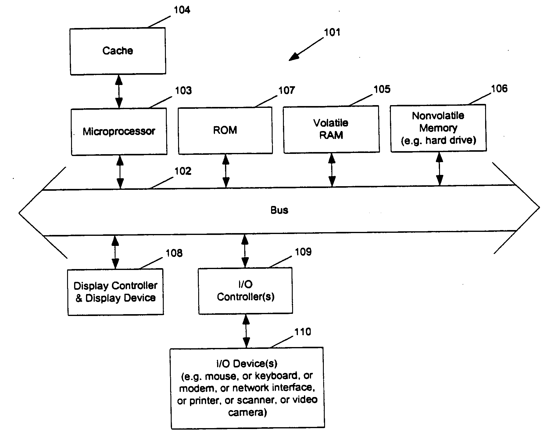
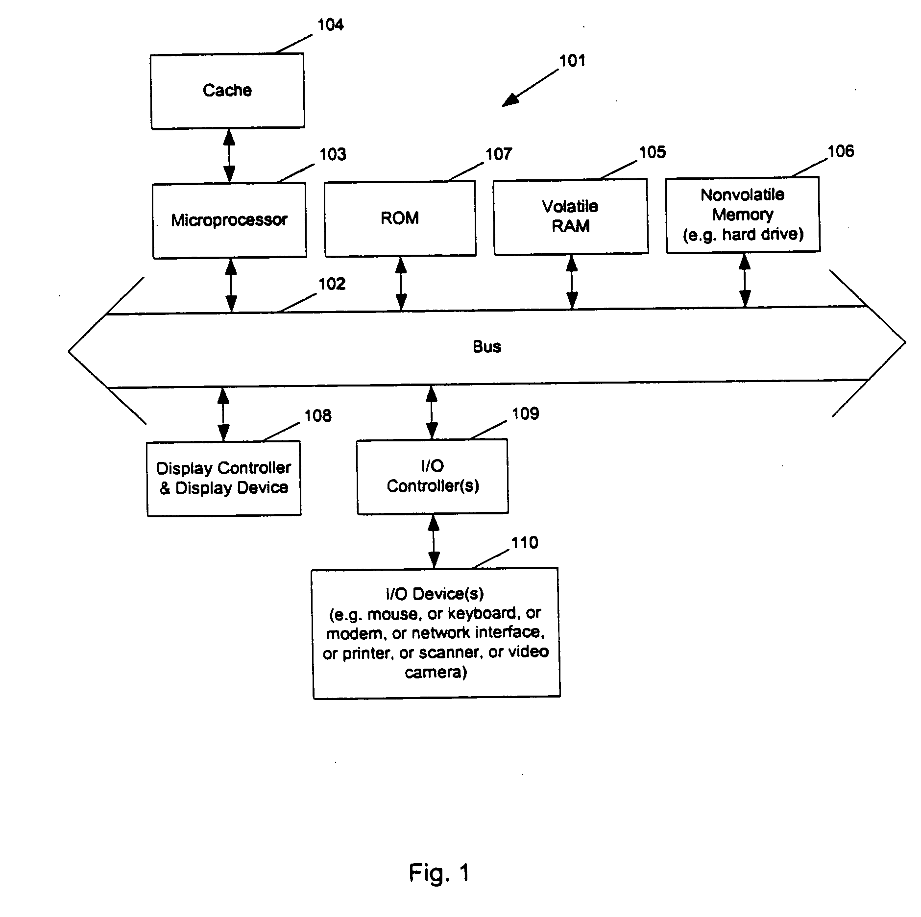
[0071]FIG. 1 shows one example of a typical computer system which may be used with the present invention. Note that while FIG. 1 illustrates various components of a computer system, it is not intended to represent any particular architecture or manner of interconnecting the components as such details are not germane to the present inventi...


PUM


Abstract

Methods and apparatuses to design an Integrated Circuit (IC) with a shielding of wires. In at least one embodiment, a shielding mesh of at least two reference voltages (e.g., power and ground) is used to reduce both the capacitive coupling and the inductive coupling in routed signal wires in IC chips. In some embodiments, a type of shielding mesh (e.g., a shielding mesh with a window surrounded by a power ring, or a window with a parser set of shielding wires) is selected to make more routing area available in locally congested areas. In other embodiments, the shielding mesh is used to create or add bypass capacitance. Other embodiments are also disclosed.

Description

[0001] This application is a continuation-in-part of U.S. patent application Ser. No. 10 / 626,031, filed Jul. 23, 2003, which is related to and claims the benefit of the filing date of U.S. provisional application Ser. No. 60 / 399,760, filed Jul. 29, 2002, and entitled “Method and Apparatus for Designing Integrated Circuit Devices with Shielding” by the inventor Kenneth S. McElvain.FIELD OF THE INVENTION [0002] The invention relates to designing integrated circuits, and more particularly to shielding wires from capacitive and inductive coupling. BACKGROUND OF THE INVENTION [0003] Integrated Circuits (ICs) are used in numerous applications, such as cellular phones, wristwatch cameras, and hand-held organizers, and others. As the commercial markets and consumer demands for smaller Integrated Circuits grow, IC size requirement trends continue towards a small form factor and lowered power consumption. [0004] For the design of digital circuits on the scale of VLSI (very large scale integra...

Claims


Application Information

Patent Timeline
Patent Type & Authority Applications(United States)
IPC IPC(8): G06F17/50H01L23/552
CPCG06F17/5077H01L23/5225H01L2924/3011H01L25/00H01L2924/0002H01L2924/00G06F30/394
Inventor MCELVAIN, KENNETH S.HALPIN, WILLIAM
Owner SYNOPSYS INC
Why Eureka
Try Eureka