Thin film integrated circuit and method for manufacturing the same, CPU, memory, electronic card and electronic device

a technology of integrated circuits and thin films, applied in the direction of semiconductor devices, electrical devices, transistors, etc., can solve the problems of insufficient parasitic insufficient alignment errors, and so as to prevent shrinkage of glass substrates, reduce the resistance of source and drain regions, and form efficiently

Inactive Publication Date: 2007-10-30
SEMICON ENERGY LAB CO LTD
View PDF53 Cites 27 Cited by
  • Summary
  • Abstract
  • Description
  • Claims
  • Application Information

AI Technical Summary

Benefits of technology

[0007]The present invention has been made in view of the above problems. It is an object of the present invention to prevent shrinkage of a glass substrate and to manufacture a TFT on the glass substrate using a salicide process. Further, it is another object of the present invention to reduce resistance of source and drain regions of the TFT formed over the glass substrate.
[0008]The present invention provides a silicification (silicide) process that is applicable to a thin film integrated circuit over a glass substrate. In addition, the present invention also provides a process in which silicide can be formed efficiently by one-time annealing. Note that a thin film integrated circuit according to the present invention includes a TFT.
[0009]One feature of the present invention is that laser annealing is employed in conducting a silicification process to a thin film integrated circuit over a glass substrate. The glass substrate can be heated locally by laser annealing and thus a problem of a substrate shrinkage is solved.
[0010]In addition, a metal film is formed as a base film so as to increase laser absorption efficiency of a transparent glass substrate (hereinafter, referred to as a base metal film).
[0011]By using laser annealing, which can locally heat a glass substrate, in a silicification process, shrinkage of a substrate does not become a problem and parasitic capacitance of source and drain regions is reduced and thus, high speed operation of a thin film integrated circuit formed over a glass substrate is possible. Further, since a base metal film absorbs heat of laser irradiation, a semiconductor layer is supplied with heat from the base metal film in addition to laser irradiation, and thus efficiency of silicide of the source and drain regions can be increased. The temperature change of the semiconductor film is caused at a slower pace than the case where the base metal film is not provided. By the slow temperature change of the semiconductor film, a silicide reaction in the source and drains region proceeds, and lower resistance of the source and drain regions is achieved.
[0012]According to the present invention, a glass substrate that is larger and more inexpensive than a silicon wafer can be used and thus, thin film integrated circuits can be mass-produced at lower cost and with higher throughput and the production cost can be drastically reduced. In addition, a substrate can be used repeatedly in the case of adopting a process of fixing a thin film integrated circuit onto a flexible substrate from a glass substrate. Therefore, the cost of a thin film integrated circuit can be reduced.

Problems solved by technology

Therefore, shrinkage of the glass substrate is caused and alignment error becomes a problem.
However, since the reaction is finished just when the high-resistant phase TiSi2 is formed, parasitic resistance of the source and drain regions is not sufficiently reduced.

Method used


Image

  • Thin film integrated circuit and method for manufacturing the same, CPU, memory, electronic card and electronic device
  • Thin film integrated circuit and method for manufacturing the same, CPU, memory, electronic card and electronic device
  • Thin film integrated circuit and method for manufacturing the same, CPU, memory, electronic card and electronic device

Examples


embodiment mode 1

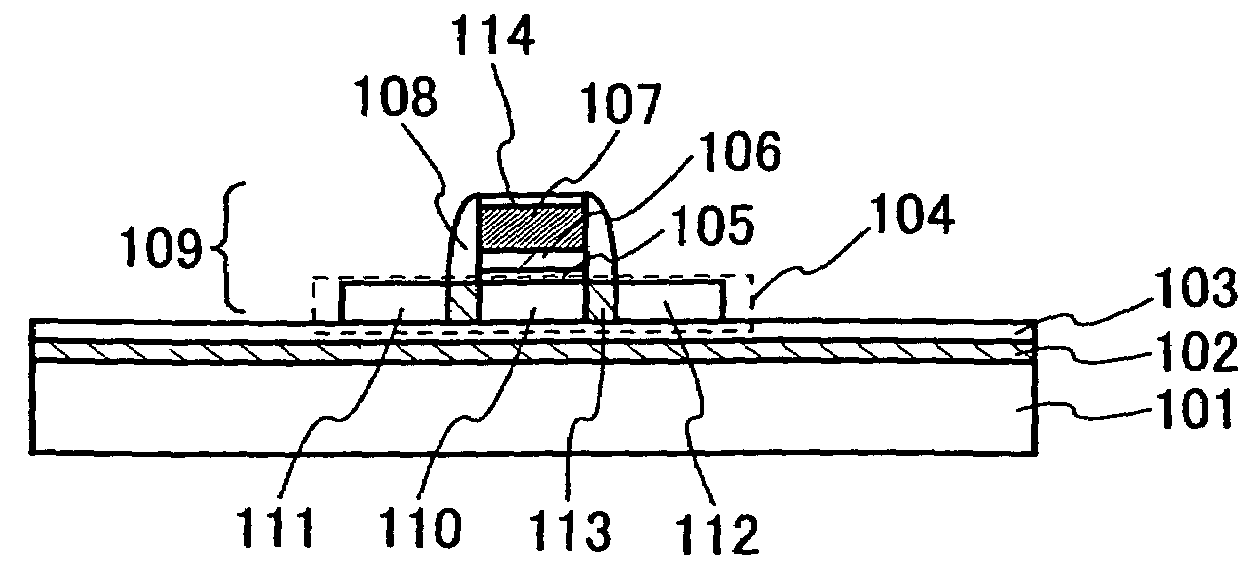
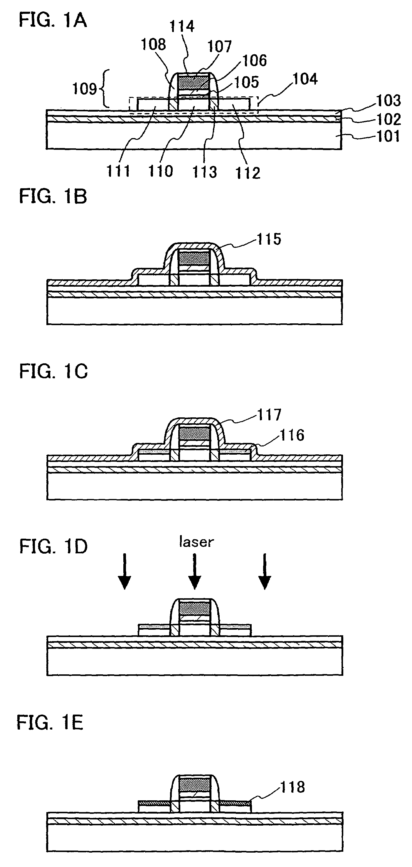
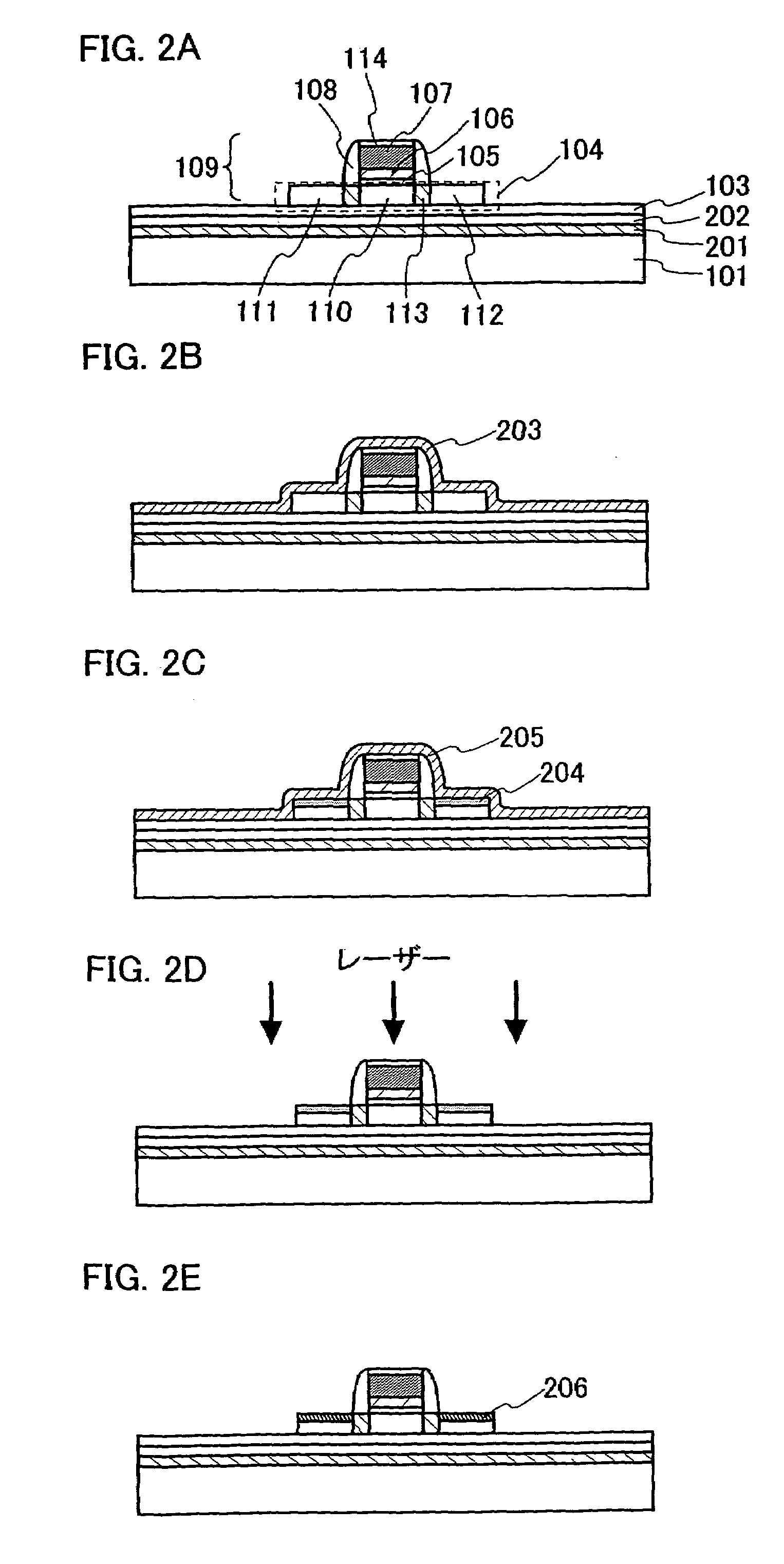
[0027]Embodiment Mode 1 describes a salicide process in the case of using a metal for a base film of a thin film integrated circuit. First, the present inventors have examined whether which stage in a salicide process using two-step annealing is effective for conducting laser annealing.

[0028]If second annealing for obtaining a low-resistant silicide is conducted simultaneously to the whole surface of a substrate, annealing at high-temperature of e.g., 800 to 850° C. is needed and thus shrinkage of a glass substrate becomes a problem. In view of the problem, a laser is used for the second annealing so as to locally heat the glass substrate. In this case, shrinkage of the glass substrate is not a problem; however, since laser annealing is conducted after selectively removing an unreacted metal film, the metal film as a heat-absorption layer is reduced more than in the first annealing. Thus, it is conceivable that laser absorption efficiency is low and a silicide reaction is difficult ...

embodiment mode 2

[0036]Embodiment Mode 2 describes a mode where the salicide process described in Embodiment Mode 1 is applied to a process of fixing a thin film integrated circuit to a flexible substrate such as plastic.

[0037]As a substrate over which a separation layer including a thin film integrated circuit, a glass substrate, a quartz substrate, a semiconductor substrate, a ceramic substrate, a metal substrate or the like can be used, and a glass substrate is used in this embodiment mode. This is because a glass substrate is more inexpensive than the other substrates and further, the size of the substrate can be enlarged. Therefore, a plurality of display devices or thin film integrated circuits can be manufactured simultaneously from one large glass substrate, and display devices or thin film integrated circuits can be mass-produced at a lower cost with higher throughput. Moreover, a glass substrate can be applied to a lager and larger screen of a display device.

[0038]Hereinafter, this embodim...

embodiment mode 3

[0053]Embodiment Mode 3 describes a mode where a silicification process can be conducted efficiently by one-time annealing in a thin film integrated circuit over a glass substrate with reference to FIGS. 4A to 4D. Note that a TFT having a sidewall over the glass substrate is identical to that of Embodiment Mode 1, and thus the description thereof is omitted and shown by the same reference numeral.

[0054]A metal film 401 is formed to cover the TFT 109, and a resist 402 is formed over source and drain regions to be silicified (FIG. 4A). The metal film 401 is selectively removed by a mixed solution of ammonia water and hydrogen peroxide solution or the like, thereby partially leaving the metal film 403 over the source and drain regions as shown in FIG. 4B. Then, silicification of the source and drain regions is conducted by laser annealing (FIG. 4C). An excimer laser, a solid-state laser (wavelength: 1064 nm or 532 nm) and the like can be used. If the TFT 109 is formed on the front surf...


PUM

PropertyMeasurementUnit
temperatureaaaaaaaaaa

Abstract

A salicide process is conducted to a thin film integrated circuit without worrying about damages to a glass substrate, and thus, high-speed operation of a circuit can be achieved. A base metal film, an oxide and a base insulating film are formed over a glass substrate. A TFT having a sidewall is formed over the base insulating film, and a metal film is formed to cover the TFT. Annealing is conducted by RTA or the like at such a temperature that does not cause shrinkage of the substrate, and a high-resistant metal silicide layer is formed in source and drain regions. After removing an unreacted metal film, laser irradiation is conducted for the second annealing; therefore a silicide reaction proceeds and the high-resistant metal silicide layer becomes a low-resistant metal silicide layer. In the second annealing, a base metal film absorbs and accumulates heat of the laser irradiation, and a semiconductor layer is supplied with heat of the base metal film in addition to heat of the laser irradiation, thereby enhancing efficiency of the silicide reaction in the source and drain regions.

Description

BACKGROUND OF THE INVENTION[0001]1. Field of the Invention[0002]The present invention relates to a thin film transistor (hereinafter, referred to as a TFT) formed over an insulating substrate such as glass, and a thin film integrated circuit including a plurality of TFTs, and a method for manufacturing the same.[0003]2. Description of the Related Art[0004]In order to realize high speed operation of a circuit, in a large scale integrated circuit (hereinafter, also referred to as an LSI) using a Si-wafer, a silicide is used for a source region, a drain region, and a gate electrode to lower resistance of the source region and drain region, and thus contact resistance is reduced. Salicide (Self Align Silicide) is known as a process for forming a silicide in a self-aligned manner with a diffusion layer of a MOS transistor (for example, Reference 1: Innovation of Logic LSI technology edited by Kenji Maeguchi, Masao Fukuma, Sotoju Asai, Science Forum pp. 238-241.)[0005]FIGS. 5A to 5D each ...

Claims


Application Information

Patent Timeline
Patent Type & Authority Patents(United States)
IPC IPC(8): H01L21/44H01L21/00H01L21/77H01L21/84H01L27/12
CPCH01L27/1214H01L27/1259
Inventor YAMAGUCHI, TETSUJIISOBE, ATSUOSAITO, SATORU
Owner SEMICON ENERGY LAB CO LTD
Why Eureka
Try Eureka